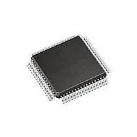
AT90CAN128-15AZ Atmel, AT90CAN128-15AZ Datasheet - Page 153

AT90CAN128-15AZ
Manufacturer Part Number
AT90CAN128-15AZ
Description
MCU AVR 128K FLASH 15MHZ 64TQFP
Manufacturer
Atmel
Series
AVR® 90CANr
Specifications of AT90CAN128-15AZ
Package / Case
64-TQFP, 64-VQFP
Voltage - Supply (vcc/vdd)
2.7 V ~ 5.5 V
Operating Temperature
-40°C ~ 125°C
Speed
16MHz
Number Of I /o
53
Eeprom Size
4K x 8
Core Processor
AVR
Program Memory Type
FLASH
Ram Size
4K x 8
Program Memory Size
128KB (128K x 8)
Data Converters
A/D 8x10b
Oscillator Type
Internal
Peripherals
Brown-out Detect/Reset, POR, PWM, WDT
Connectivity
CAN, I²C, SPI, UART/USART
Core Size
8-Bit
Processor Series
AT90CANx
Core
AVR8
Data Bus Width
8 bit
Data Ram Size
4 KB
Interface Type
CAN, SPI, UART
Maximum Clock Frequency
16 MHz
Number Of Programmable I/os
53
Number Of Timers
4
Maximum Operating Temperature
+ 125 C
Mounting Style
SMD/SMT
3rd Party Development Tools
EWAVR, EWAVR-BL
Development Tools By Supplier
ATAVRDRAGON, ATSTK500, ATSTK600, ATAVRISP2, ATDVK90CAN1, ATADAPCAN01
Minimum Operating Temperature
- 40 C
On-chip Adc
10 bit, 8 Channel
Cpu Family
90C
Device Core
AVR
Device Core Size
8b
Frequency (max)
16MHz
Total Internal Ram Size
4KB
# I/os (max)
53
Number Of Timers - General Purpose
4
Operating Supply Voltage (typ)
3.3/5V
Operating Supply Voltage (max)
5.5V
Operating Supply Voltage (min)
2.7V
Instruction Set Architecture
RISC
Operating Temp Range
-40C to 125C
Operating Temperature Classification
Automotive
Mounting
Surface Mount
Pin Count
64
Package Type
TQFP
Lead Free Status / RoHS Status
Lead free / RoHS Compliant
Available stocks
Company
Part Number
Manufacturer
Quantity
Price
Company:
Part Number:
AT90CAN128-15AZ
Manufacturer:
SAMSUNG
Quantity:
1 001
Company:
Part Number:
AT90CAN128-15AZ
Manufacturer:
ATMEL
Quantity:
1 000
Part Number:
AT90CAN128-15AZ
Manufacturer:
ATMEL/爱特梅尔
Quantity:
20 000
- Current page: 153 of 428
- Download datasheet (6Mb)
14.7.4
7679H–CAN–08/08
Phase Correct PWM Mode
The Timer/Counter Overflow Flag (TOV2) is set each time the counter reaches MAX. If the inter-
rupt is enabled, the interrupt handler routine can be used for updating the compare value.
In fast PWM mode, the compare unit allows generation of PWM waveforms on the OC2A pin.
Setting the COM2A1:0 bits to two will produce a non-inverted PWM and an inverted PWM output
can be generated by setting the COM2A1:0 to three (See
OC2A value will only be visible on the port pin if the data direction for the port pin is set as out-
put. The PWM waveform is generated by setting (or clearing) the OC2A Register at the compare
match between OCR2A and TCNT2, and clearing (or setting) the OC2A Register at the timer
clock cycle the counter is cleared (changes from MAX to BOTTOM).
The PWM frequency for the output can be calculated by the following equation:
The N variable represents the prescale factor (1, 8, 32, 64, 128, 256, or 1024).
The extreme values for the OCR2A Register represent special cases when generating a PWM
waveform output in the fast PWM mode. If the OCR2A is set equal to BOTTOM, the output will
be a narrow spike for each MAX+1 timer clock cycle. Setting the OCR2A equal to MAX will result
in a constantly high or low output (depending on the polarity of the output set by the COM2A1:0
bits.)
A frequency (with 50% duty cycle) waveform output in fast PWM mode can be achieved by set-
ting OC2A to toggle its logical level on each compare match (COM2A1:0 = 1). The waveform
generated will have a maximum frequency of f
feature is similar to the OC2A toggle in CTC mode, except the double buffer feature of the Out-
put Compare unit is enabled in the fast PWM mode.
The phase correct PWM mode (WGM21:0 = 1) provides a high resolution phase correct PWM
waveform generation option. The phase correct PWM mode is based on a dual-slope operation.
The counter counts repeatedly from BOTTOM to MAX and then from MAX to BOTTOM. In non-
inverting Compare Output mode, the Output Compare (OC2A) is cleared on the compare match
between TCNT2 and OCR2A while upcounting, and set on the compare match while down-
counting. In inverting Output Compare mode, the operation is inverted. The dual-slope operation
has lower maximum operation frequency than single slope operation. However, due to the sym-
metric feature of the dual-slope PWM modes, these modes are preferred for motor control
applications.
The PWM resolution for the phase correct PWM mode is fixed to eight bits. In phase correct
PWM mode the counter is incremented until the counter value matches MAX. When the counter
reaches MAX, it changes the count direction. The TCNT2 value will be equal to MAX for one
timer clock cycle. The timing diagram for the phase correct PWM mode is shown on
The TCNT2 value is in the timing diagram shown as a histogram for illustrating the dual-slope
operation. The diagram includes non-inverted and inverted PWM outputs. The small horizontal
line marks on the TCNT2 slopes represent compare matches between OCR2A and TCNT2.
f
OCnxPWM
oc2A
=
= f
----------------- -
N 256
clk_I/O
f
clk_I/O
⋅
Table 14-3 on page
AT90CAN32/64/128
/2 when OCR2A is set to zero. This
158). The actual
Figure
14-8.
153
Related parts for AT90CAN128-15AZ
Image
Part Number
Description
Manufacturer
Datasheet
Request
R

Part Number:
Description:
DEV KIT FOR AVR/AVR32
Manufacturer:
Atmel
Datasheet:

Part Number:
Description:
INTERVAL AND WIPE/WASH WIPER CONTROL IC WITH DELAY
Manufacturer:
ATMEL Corporation
Datasheet:

Part Number:
Description:
Low-Voltage Voice-Switched IC for Hands-Free Operation
Manufacturer:
ATMEL Corporation
Datasheet:

Part Number:
Description:
MONOLITHIC INTEGRATED FEATUREPHONE CIRCUIT
Manufacturer:
ATMEL Corporation
Datasheet:

Part Number:
Description:
AM-FM Receiver IC U4255BM-M
Manufacturer:
ATMEL Corporation
Datasheet:

Part Number:
Description:
Monolithic Integrated Feature Phone Circuit
Manufacturer:
ATMEL Corporation
Datasheet:

Part Number:
Description:
Multistandard Video-IF and Quasi Parallel Sound Processing
Manufacturer:
ATMEL Corporation
Datasheet:

Part Number:
Description:
High-performance EE PLD
Manufacturer:
ATMEL Corporation
Datasheet:

Part Number:
Description:
8-bit Flash Microcontroller
Manufacturer:
ATMEL Corporation
Datasheet:

Part Number:
Description:
2-Wire Serial EEPROM
Manufacturer:
ATMEL Corporation
Datasheet:


