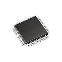
AT90CAN128-15AZ Atmel, AT90CAN128-15AZ Datasheet - Page 303

AT90CAN128-15AZ
Manufacturer Part Number
AT90CAN128-15AZ
Description
MCU AVR 128K FLASH 15MHZ 64TQFP
Manufacturer
Atmel
Series
AVR® 90CANr
Specifications of AT90CAN128-15AZ
Package / Case
64-TQFP, 64-VQFP
Voltage - Supply (vcc/vdd)
2.7 V ~ 5.5 V
Operating Temperature
-40°C ~ 125°C
Speed
16MHz
Number Of I /o
53
Eeprom Size
4K x 8
Core Processor
AVR
Program Memory Type
FLASH
Ram Size
4K x 8
Program Memory Size
128KB (128K x 8)
Data Converters
A/D 8x10b
Oscillator Type
Internal
Peripherals
Brown-out Detect/Reset, POR, PWM, WDT
Connectivity
CAN, I²C, SPI, UART/USART
Core Size
8-Bit
Processor Series
AT90CANx
Core
AVR8
Data Bus Width
8 bit
Data Ram Size
4 KB
Interface Type
CAN, SPI, UART
Maximum Clock Frequency
16 MHz
Number Of Programmable I/os
53
Number Of Timers
4
Maximum Operating Temperature
+ 125 C
Mounting Style
SMD/SMT
3rd Party Development Tools
EWAVR, EWAVR-BL
Development Tools By Supplier
ATAVRDRAGON, ATSTK500, ATSTK600, ATAVRISP2, ATDVK90CAN1, ATADAPCAN01
Minimum Operating Temperature
- 40 C
On-chip Adc
10 bit, 8 Channel
Cpu Family
90C
Device Core
AVR
Device Core Size
8b
Frequency (max)
16MHz
Total Internal Ram Size
4KB
# I/os (max)
53
Number Of Timers - General Purpose
4
Operating Supply Voltage (typ)
3.3/5V
Operating Supply Voltage (max)
5.5V
Operating Supply Voltage (min)
2.7V
Instruction Set Architecture
RISC
Operating Temp Range
-40C to 125C
Operating Temperature Classification
Automotive
Mounting
Surface Mount
Pin Count
64
Package Type
TQFP
Lead Free Status / RoHS Status
Lead free / RoHS Compliant
Available stocks
Company
Part Number
Manufacturer
Quantity
Price
Company:
Part Number:
AT90CAN128-15AZ
Manufacturer:
SAMSUNG
Quantity:
1 001
Company:
Part Number:
AT90CAN128-15AZ
Manufacturer:
ATMEL
Quantity:
1 000
Part Number:
AT90CAN128-15AZ
Manufacturer:
ATMEL/爱特梅尔
Quantity:
20 000
- Current page: 303 of 428
- Download datasheet (6Mb)
23.4.1
23.4.2
23.4.3
23.4.4
23.4.5
7679H–CAN–08/08
EXTEST (0x0)
IDCODE (0x1)
SAMPLE_PRELOAD (0x2)
AVR_RESET (0xC)
BYPASS (0xF)
Mandatory JTAG instruction for selecting the Boundary-scan Chain as data register for testing
circuitry external to the AVR package. For port-pins, Pull-up Disable, Output Control, Output
Data, and Input Data are all accessible in the scan chain. For Analog circuits having off-chip
connections, the interface between the analog and the digital logic is in the scan chain. The con-
tents of the latched outputs of the Boundary-scan chain is driven out as soon as the JTAG IR-
Register is loaded with the EXTEST instruction.
The active states are:
Optional JTAG instruction selecting the 32 bit ID-Register as data register. The ID-Register con-
sists of a version number, a device number and the manufacturer code chosen by JEDEC. This
is the default instruction after power-up.
The active states are:
Mandatory JTAG instruction for pre-loading the output latches and taking a snap-shot of the
input/output pins without affecting the system operation. However, the output latches are not
connected to the pins. The Boundary-scan Chain is selected as data register.
The active states are:
The AVR specific public JTAG instruction for forcing the AVR device into the Reset mode or
releasing the JTAG reset source. The TAP controller is not reset by this instruction. The one bit
Reset Register is selected as data register.
Note that the reset will be active as long as there is a logic “one” in the Reset Chain.
The output from this chain is not latched.
The active states are:
Mandatory JTAG instruction selecting the Bypass Register for data register.
The active states are:
• Capture-DR: Data on the external pins are sampled into the Boundary-scan Chain.
• Shift-DR: The Internal Scan Chain is shifted by the TCK input.
• Update-DR: Data from the scan chain is applied to output pins.
• Capture-DR: Data in the IDCODE Register is sampled into the Boundary-scan Chain.
• Shift-DR: The IDCODE scan chain is shifted by the TCK input.
• Capture-DR: Data on the external pins are sampled into the Boundary-scan Chain.
• Shift-DR: The Boundary-scan Chain is shifted by the TCK input.
• Update-DR: Data from the Boundary-scan chain is applied to the output latches. However,
• Shift-DR: The Reset Register is shifted by the TCK input.
• Capture-DR: Loads a logic “0” into the Bypass Register.
the output latches are not connected to the pins.
AT90CAN32/64/128
303
Related parts for AT90CAN128-15AZ
Image
Part Number
Description
Manufacturer
Datasheet
Request
R

Part Number:
Description:
DEV KIT FOR AVR/AVR32
Manufacturer:
Atmel
Datasheet:

Part Number:
Description:
INTERVAL AND WIPE/WASH WIPER CONTROL IC WITH DELAY
Manufacturer:
ATMEL Corporation
Datasheet:

Part Number:
Description:
Low-Voltage Voice-Switched IC for Hands-Free Operation
Manufacturer:
ATMEL Corporation
Datasheet:

Part Number:
Description:
MONOLITHIC INTEGRATED FEATUREPHONE CIRCUIT
Manufacturer:
ATMEL Corporation
Datasheet:

Part Number:
Description:
AM-FM Receiver IC U4255BM-M
Manufacturer:
ATMEL Corporation
Datasheet:

Part Number:
Description:
Monolithic Integrated Feature Phone Circuit
Manufacturer:
ATMEL Corporation
Datasheet:

Part Number:
Description:
Multistandard Video-IF and Quasi Parallel Sound Processing
Manufacturer:
ATMEL Corporation
Datasheet:

Part Number:
Description:
High-performance EE PLD
Manufacturer:
ATMEL Corporation
Datasheet:

Part Number:
Description:
8-bit Flash Microcontroller
Manufacturer:
ATMEL Corporation
Datasheet:

Part Number:
Description:
2-Wire Serial EEPROM
Manufacturer:
ATMEL Corporation
Datasheet:


