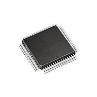
AT90CAN128-15AZ Atmel, AT90CAN128-15AZ Datasheet - Page 308

AT90CAN128-15AZ
Manufacturer Part Number
AT90CAN128-15AZ
Description
MCU AVR 128K FLASH 15MHZ 64TQFP
Manufacturer
Atmel
Series
AVR® 90CANr
Specifications of AT90CAN128-15AZ
Package / Case
64-TQFP, 64-VQFP
Voltage - Supply (vcc/vdd)
2.7 V ~ 5.5 V
Operating Temperature
-40°C ~ 125°C
Speed
16MHz
Number Of I /o
53
Eeprom Size
4K x 8
Core Processor
AVR
Program Memory Type
FLASH
Ram Size
4K x 8
Program Memory Size
128KB (128K x 8)
Data Converters
A/D 8x10b
Oscillator Type
Internal
Peripherals
Brown-out Detect/Reset, POR, PWM, WDT
Connectivity
CAN, I²C, SPI, UART/USART
Core Size
8-Bit
Processor Series
AT90CANx
Core
AVR8
Data Bus Width
8 bit
Data Ram Size
4 KB
Interface Type
CAN, SPI, UART
Maximum Clock Frequency
16 MHz
Number Of Programmable I/os
53
Number Of Timers
4
Maximum Operating Temperature
+ 125 C
Mounting Style
SMD/SMT
3rd Party Development Tools
EWAVR, EWAVR-BL
Development Tools By Supplier
ATAVRDRAGON, ATSTK500, ATSTK600, ATAVRISP2, ATDVK90CAN1, ATADAPCAN01
Minimum Operating Temperature
- 40 C
On-chip Adc
10 bit, 8 Channel
Cpu Family
90C
Device Core
AVR
Device Core Size
8b
Frequency (max)
16MHz
Total Internal Ram Size
4KB
# I/os (max)
53
Number Of Timers - General Purpose
4
Operating Supply Voltage (typ)
3.3/5V
Operating Supply Voltage (max)
5.5V
Operating Supply Voltage (min)
2.7V
Instruction Set Architecture
RISC
Operating Temp Range
-40C to 125C
Operating Temperature Classification
Automotive
Mounting
Surface Mount
Pin Count
64
Package Type
TQFP
Lead Free Status / RoHS Status
Lead free / RoHS Compliant
Available stocks
Company
Part Number
Manufacturer
Quantity
Price
Company:
Part Number:
AT90CAN128-15AZ
Manufacturer:
SAMSUNG
Quantity:
1 001
Company:
Part Number:
AT90CAN128-15AZ
Manufacturer:
ATMEL
Quantity:
1 000
Part Number:
AT90CAN128-15AZ
Manufacturer:
ATMEL/爱特梅尔
Quantity:
20 000
- Current page: 308 of 428
- Download datasheet (6Mb)
23.6.5
308
AT90CAN32/64/128
Scanning the Analog Comparator
Figure 23-7. Boundary-scan Cells for Oscillators and Clock Options
Table 23-5
XTAL1/XTAL2 connections as well as external Timer2 clock pin TOSC1 and 32kHz Timer2
Oscillator.
Table 23-5.
Notes:
The relevant Comparator signals regarding Boundary-scan are shown in
Boundary-scan cell from
described in
The Comparator need not be used for pure connectivity testing, since all analog inputs are
shared with a digital port pin as well.
Enable Signal
EXTCLKEN
OSCON
OSC32EN
TOSKON
1. Do not enable more than one clock source as clock at a time.
2. Scanning an Oscillator output gives unpredictable results as there is a frequency drift between
3. The main clock configuration is programmed by fuses. As a fuse is not changed run-time, the
From Digital Logic
the internal Oscillator and the JTAG TCK clock. If possible, scanning an external clock is
preferred.
main clock configuration is considered fixed for a given application. The user is advised to
scan the same clock option as to be used in the final system. The enable signals are sup-
ported in the scan chain because the system logic can disable clock options in sleep modes,
thereby disconnecting the Oscillator pins from the scan path if not provided.
summaries the scan registers for the external clock pin XTAL1, oscillators with
Table
Scan Signals for the Oscillators
Scanned Clock Line
EXTCLK (XTAL1)
OSCCK
OSC32CK
TOSCK
23-6.
Previous
From
Cell
ShiftDR
0
1
ClockDR
Figure 23-9
D
UpdateDR
Q
Next
Cell
To
D
G
is attached to each of these signals. The signals are
Q
Clock Option
External Main Clock
External Crystal
External Ceramic Resonator
Low Freq. External Crystal
32 kHz Timer2 Oscillator
EXTEST
0
1
(1)(2)(3)
XTAL1 / TOSC1
ENABLE
Oscillator
XTAL2 / TOSC2
OUTPUT
Previous
From
Cell
ShiftDR
0
1
ClockDR
Scanned Clock Line
when not Used
D
Figure
FF1
Q
Next
Cell
To
7679H–CAN–08/08
0
1
1
1
23-8. The
To System Logic
Related parts for AT90CAN128-15AZ
Image
Part Number
Description
Manufacturer
Datasheet
Request
R

Part Number:
Description:
DEV KIT FOR AVR/AVR32
Manufacturer:
Atmel
Datasheet:

Part Number:
Description:
INTERVAL AND WIPE/WASH WIPER CONTROL IC WITH DELAY
Manufacturer:
ATMEL Corporation
Datasheet:

Part Number:
Description:
Low-Voltage Voice-Switched IC for Hands-Free Operation
Manufacturer:
ATMEL Corporation
Datasheet:

Part Number:
Description:
MONOLITHIC INTEGRATED FEATUREPHONE CIRCUIT
Manufacturer:
ATMEL Corporation
Datasheet:

Part Number:
Description:
AM-FM Receiver IC U4255BM-M
Manufacturer:
ATMEL Corporation
Datasheet:

Part Number:
Description:
Monolithic Integrated Feature Phone Circuit
Manufacturer:
ATMEL Corporation
Datasheet:

Part Number:
Description:
Multistandard Video-IF and Quasi Parallel Sound Processing
Manufacturer:
ATMEL Corporation
Datasheet:

Part Number:
Description:
High-performance EE PLD
Manufacturer:
ATMEL Corporation
Datasheet:

Part Number:
Description:
8-bit Flash Microcontroller
Manufacturer:
ATMEL Corporation
Datasheet:

Part Number:
Description:
2-Wire Serial EEPROM
Manufacturer:
ATMEL Corporation
Datasheet:


