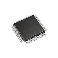
AT90CAN128-15AZ Atmel, AT90CAN128-15AZ Datasheet - Page 195

AT90CAN128-15AZ
Manufacturer Part Number
AT90CAN128-15AZ
Description
MCU AVR 128K FLASH 15MHZ 64TQFP
Manufacturer
Atmel
Series
AVR® 90CANr
Specifications of AT90CAN128-15AZ
Package / Case
64-TQFP, 64-VQFP
Voltage - Supply (vcc/vdd)
2.7 V ~ 5.5 V
Operating Temperature
-40°C ~ 125°C
Speed
16MHz
Number Of I /o
53
Eeprom Size
4K x 8
Core Processor
AVR
Program Memory Type
FLASH
Ram Size
4K x 8
Program Memory Size
128KB (128K x 8)
Data Converters
A/D 8x10b
Oscillator Type
Internal
Peripherals
Brown-out Detect/Reset, POR, PWM, WDT
Connectivity
CAN, I²C, SPI, UART/USART
Core Size
8-Bit
Processor Series
AT90CANx
Core
AVR8
Data Bus Width
8 bit
Data Ram Size
4 KB
Interface Type
CAN, SPI, UART
Maximum Clock Frequency
16 MHz
Number Of Programmable I/os
53
Number Of Timers
4
Maximum Operating Temperature
+ 125 C
Mounting Style
SMD/SMT
3rd Party Development Tools
EWAVR, EWAVR-BL
Development Tools By Supplier
ATAVRDRAGON, ATSTK500, ATSTK600, ATAVRISP2, ATDVK90CAN1, ATADAPCAN01
Minimum Operating Temperature
- 40 C
On-chip Adc
10 bit, 8 Channel
Cpu Family
90C
Device Core
AVR
Device Core Size
8b
Frequency (max)
16MHz
Total Internal Ram Size
4KB
# I/os (max)
53
Number Of Timers - General Purpose
4
Operating Supply Voltage (typ)
3.3/5V
Operating Supply Voltage (max)
5.5V
Operating Supply Voltage (min)
2.7V
Instruction Set Architecture
RISC
Operating Temp Range
-40C to 125C
Operating Temperature Classification
Automotive
Mounting
Surface Mount
Pin Count
64
Package Type
TQFP
Lead Free Status / RoHS Status
Lead free / RoHS Compliant
Available stocks
Company
Part Number
Manufacturer
Quantity
Price
Company:
Part Number:
AT90CAN128-15AZ
Manufacturer:
SAMSUNG
Quantity:
1 001
Company:
Part Number:
AT90CAN128-15AZ
Manufacturer:
ATMEL
Quantity:
1 000
Part Number:
AT90CAN128-15AZ
Manufacturer:
ATMEL/爱特梅尔
Quantity:
20 000
- Current page: 195 of 428
- Download datasheet (6Mb)
17.11 USART Register Description
17.11.1
17.11.2
17.11.3
17.11.4
7679H–CAN–08/08
USART0 I/O Data Register – UDR0
USART1 I/O Data Register – UDR1
USART0 Control and Status Register A – UCSR0A
USART1 Control and Status Register A – UCSR1A
• Bit 7:0 – RxBn7:0: Receive Data Buffer (read access)
• Bit 7:0 – TxBn7:0: Transmit Data Buffer (write access)
The USARTn Transmit Data Buffer Register and USARTn Receive Data Buffer Registers share
the same I/O address referred to as USARTn Data Register or UDRn. The Transmit Data Buffer
Register (TXBn) will be the destination for data written to the UDRn Register location. Reading
the UDRn Register location will return the contents of the Receive Data Buffer Register (RXBn).
For 5-, 6-, or 7-bit characters the upper unused bits will be ignored by the Transmitter and set to
zero by the Receiver.
The transmit buffer can only be written when the UDREn flag in the UCSRnA Register is set.
Data written to UDRn when the UDREn flag is not set, will be ignored by the USARTn Transmit-
ter. When data is written to the transmit buffer, and the Transmitter is enabled, the Transmitter
will load the data into the Transmit Shift Register when the Shift Register is empty. Then the
data will be serially transmitted on the TxDn pin.
The receive buffer consists of a two level FIFO. The FIFO will change its state whenever the
receive buffer is accessed.
• Bit 7 – RXCn: USARTn Receive Complete
This flag bit is set when there are unread data in the receive buffer and cleared when the receive
buffer is empty (i.e., does not contain any unread data). If the Receiver is disabled, the receive
buffer will be flushed and consequently the RXCn bit will become zero. The RXCn flag can be
used to generate a Receive Complete interrupt (see description of the RXCIEn bit).
Bit
Read/Write
Initial Value
Bit
Read/Write
Initial Value
Initial Value
Initial Value
Read/Write
Read/Write
Bit
Bit
RXC0
RXC1
R/W
R/W
7
0
7
0
R
R
7
0
7
0
TXC0
TXC1
R/W
R/W
R/W
R/W
6
0
6
0
6
0
6
0
UDRE0
UDRE1
R/W
R/W
5
0
5
0
R
R
5
1
5
1
R/W
R/W
FE0
FE1
4
0
4
0
4
R
0
4
R
0
RXB0[7:0]
RXB1[7:0]
TXB0[7:0]
TXB1[7:0]
R/W
R/W
DOR0
DOR1
3
0
3
0
R
R
3
0
3
0
R/W
R/W
UPE0
UPE1
2
0
2
0
R
R
2
0
2
0
AT90CAN32/64/128
R/W
R/W
U2X0
U2X1
1
0
1
0
R/W
R/W
1
0
1
0
R/W
R/W
MPCM0
MPCM1
0
0
0
0
R/W
R/W
0
0
0
0
UDR0 (Write)
UDR1 (Write)
UDR0 (Read)
UDR1 (Read)
UCSR0A
UCSR1A
195
Related parts for AT90CAN128-15AZ
Image
Part Number
Description
Manufacturer
Datasheet
Request
R

Part Number:
Description:
DEV KIT FOR AVR/AVR32
Manufacturer:
Atmel
Datasheet:

Part Number:
Description:
INTERVAL AND WIPE/WASH WIPER CONTROL IC WITH DELAY
Manufacturer:
ATMEL Corporation
Datasheet:

Part Number:
Description:
Low-Voltage Voice-Switched IC for Hands-Free Operation
Manufacturer:
ATMEL Corporation
Datasheet:

Part Number:
Description:
MONOLITHIC INTEGRATED FEATUREPHONE CIRCUIT
Manufacturer:
ATMEL Corporation
Datasheet:

Part Number:
Description:
AM-FM Receiver IC U4255BM-M
Manufacturer:
ATMEL Corporation
Datasheet:

Part Number:
Description:
Monolithic Integrated Feature Phone Circuit
Manufacturer:
ATMEL Corporation
Datasheet:

Part Number:
Description:
Multistandard Video-IF and Quasi Parallel Sound Processing
Manufacturer:
ATMEL Corporation
Datasheet:

Part Number:
Description:
High-performance EE PLD
Manufacturer:
ATMEL Corporation
Datasheet:

Part Number:
Description:
8-bit Flash Microcontroller
Manufacturer:
ATMEL Corporation
Datasheet:

Part Number:
Description:
2-Wire Serial EEPROM
Manufacturer:
ATMEL Corporation
Datasheet:


