AT90CAN128-15AZ Atmel, AT90CAN128-15AZ Datasheet - Page 48
AT90CAN128-15AZ
Manufacturer Part Number
AT90CAN128-15AZ
Description
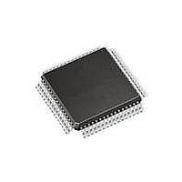
MCU AVR 128K FLASH 15MHZ 64TQFP
Manufacturer
Atmel
Series
AVR® 90CANr
Specifications of AT90CAN128-15AZ
Package / Case
64-TQFP, 64-VQFP
Voltage - Supply (vcc/vdd)
2.7 V ~ 5.5 V
Operating Temperature
-40°C ~ 125°C
Speed
16MHz
Number Of I /o
53
Eeprom Size
4K x 8
Core Processor
AVR
Program Memory Type
FLASH
Ram Size
4K x 8
Program Memory Size
128KB (128K x 8)
Data Converters
A/D 8x10b
Oscillator Type
Internal
Peripherals
Brown-out Detect/Reset, POR, PWM, WDT
Connectivity
CAN, I²C, SPI, UART/USART
Core Size
8-Bit
Processor Series
AT90CANx
Core
AVR8
Data Bus Width
8 bit
Data Ram Size
4 KB
Interface Type
CAN, SPI, UART
Maximum Clock Frequency
16 MHz
Number Of Programmable I/os
53
Number Of Timers
4
Maximum Operating Temperature
+ 125 C
Mounting Style
SMD/SMT
3rd Party Development Tools
EWAVR, EWAVR-BL
Development Tools By Supplier
ATAVRDRAGON, ATSTK500, ATSTK600, ATAVRISP2, ATDVK90CAN1, ATADAPCAN01
Minimum Operating Temperature
- 40 C
On-chip Adc
10 bit, 8 Channel
Cpu Family
90C
Device Core
AVR
Device Core Size
8b
Frequency (max)
16MHz
Total Internal Ram Size
4KB
# I/os (max)
53
Number Of Timers - General Purpose
4
Operating Supply Voltage (typ)
3.3/5V
Operating Supply Voltage (max)
5.5V
Operating Supply Voltage (min)
2.7V
Instruction Set Architecture
RISC
Operating Temp Range
-40C to 125C
Operating Temperature Classification
Automotive
Mounting
Surface Mount
Pin Count
64
Package Type
TQFP
Lead Free Status / RoHS Status
Lead free / RoHS Compliant
Available stocks
Company
Part Number
Manufacturer
Quantity
Price
Company:

Part Number:
AT90CAN128-15AZ
Manufacturer:
SAMSUNG
Quantity:
1 001
Company:
Part Number:
AT90CAN128-15AZ
Manufacturer:
ATMEL
Quantity:
1 000
Part Number:
AT90CAN128-15AZ
Manufacturer:
ATMEL/爱特梅尔
Quantity:
20 000


6.5
Table 6-2.
Notes:
6.6
6.6.1
48
Sleep
Mode
Idle
ADC Noise
Reduction
Power-
down
Power-
save
Standby
Standby Mode
1. Only recommended with external crystal or resonator selected as clock source.
2. If AS2 bit in ASSR is set.
3. Only INT3:0 or level interrupt INT7:4.
Minimizing Power Consumption
(1)
AT90CAN32/64/128
Analog to Digital Converter
clk
Active Clock Domains and Wake-up Sources in the Different Sleep Modes.
CPU
Active Clock Domains
clk
FLASH
If Timer/Counter2 is clocked asynchronously, i.e., the AS2 bit in ASSR is set, Timer/Counter2
will run during sleep. The device can wake up from either Timer Overflow or Output Compare
event from Timer/Counter2 if the corresponding Timer/Counter2 interrupt enable bits are set in
TIMSK2, and the global interrupt enable bit in SREG is set.
If the Asynchronous Timer is NOT clocked asynchronously, Power-down mode is recommended
instead of Power-save mode because the contents of the registers in the asynchronous timer
should be considered undefined after wake-up in Power-save mode if AS2 is 0.
This sleep mode basically halts all clocks except clk
modules, including Timer/Counter2 if clocked asynchronously.
When the SM2..0 bits are 110 and an External Crystal/Resonator clock option is selected, the
SLEEP instruction makes the MCU enter Standby mode. This mode is identical to Power-down
with the exception that the Oscillator is kept running. From Standby mode, the device wakes up
in 6 clock cycles.
There are several issues to consider when trying to minimize the power consumption in an AVR
controlled system. In general, sleep modes should be used as much as possible, and the sleep
mode should be selected so that as few as possible of the device’s functions are operating. All
functions not needed should be disabled. In particular, the following modules may need special
consideration when trying to achieve the lowest possible power consumption.
If enabled, the ADC will be enabled in all sleep modes. To save power, the ADC should be dis-
abled before entering any sleep mode. When the ADC is turned off and on again, the next
conversion will be an extended conversion. Refer to
273
for details on ADC operation.
clk
X
IO
clk
X
X
ADC
clk
X
X
X
(2)
ASY
Enabled
Source
Clock
Main
X
X
X
Oscillators
Enabled
Timer
Osc.
X
X
X
(2)
(2)
(2)
INT7:0
X
X
X
X
X
(3)
(3)
(3)
(3)
ASY
“Analog to Digital Converter - ADC” on page
, allowing operation only of asynchronous
Address
Match
TWI
X
X
X
X
X
Wake-up Sources
Timer
X
X
X
2
(2)
(2)
EEPROM
Ready
SPM/
X
X
7679H–CAN–08/08
ADC
X
X
Other
I/O
X
Related parts for AT90CAN128-15AZ
Image
Part Number
Description
Manufacturer
Datasheet
Request
R

Part Number:
Description:
DEV KIT FOR AVR/AVR32
Manufacturer:
Atmel
Datasheet:

Part Number:
Description:
INTERVAL AND WIPE/WASH WIPER CONTROL IC WITH DELAY
Manufacturer:
ATMEL Corporation
Datasheet:
Part Number:
Description:
Low-Voltage Voice-Switched IC for Hands-Free Operation
Manufacturer:
ATMEL Corporation
Datasheet:
Part Number:
Description:
MONOLITHIC INTEGRATED FEATUREPHONE CIRCUIT
Manufacturer:
ATMEL Corporation
Datasheet:
Part Number:
Description:
AM-FM Receiver IC U4255BM-M
Manufacturer:
ATMEL Corporation
Datasheet:
Part Number:
Description:
Monolithic Integrated Feature Phone Circuit
Manufacturer:
ATMEL Corporation
Datasheet:
Part Number:
Description:
Multistandard Video-IF and Quasi Parallel Sound Processing
Manufacturer:
ATMEL Corporation
Datasheet:
Part Number:
Description:
High-performance EE PLD
Manufacturer:
ATMEL Corporation
Datasheet:
Part Number:
Description:
8-bit Flash Microcontroller
Manufacturer:
ATMEL Corporation
Datasheet:
Part Number:
Description:
2-Wire Serial EEPROM
Manufacturer:
ATMEL Corporation
Datasheet: