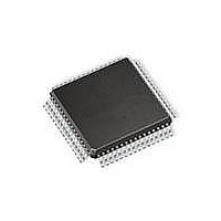
AT90CAN128-15AZ Atmel, AT90CAN128-15AZ Datasheet - Page 338

AT90CAN128-15AZ
Manufacturer Part Number
AT90CAN128-15AZ
Description
MCU AVR 128K FLASH 15MHZ 64TQFP
Manufacturer
Atmel
Series
AVR® 90CANr
Specifications of AT90CAN128-15AZ
Package / Case
64-TQFP, 64-VQFP
Voltage - Supply (vcc/vdd)
2.7 V ~ 5.5 V
Operating Temperature
-40°C ~ 125°C
Speed
16MHz
Number Of I /o
53
Eeprom Size
4K x 8
Core Processor
AVR
Program Memory Type
FLASH
Ram Size
4K x 8
Program Memory Size
128KB (128K x 8)
Data Converters
A/D 8x10b
Oscillator Type
Internal
Peripherals
Brown-out Detect/Reset, POR, PWM, WDT
Connectivity
CAN, I²C, SPI, UART/USART
Core Size
8-Bit
Processor Series
AT90CANx
Core
AVR8
Data Bus Width
8 bit
Data Ram Size
4 KB
Interface Type
CAN, SPI, UART
Maximum Clock Frequency
16 MHz
Number Of Programmable I/os
53
Number Of Timers
4
Maximum Operating Temperature
+ 125 C
Mounting Style
SMD/SMT
3rd Party Development Tools
EWAVR, EWAVR-BL
Development Tools By Supplier
ATAVRDRAGON, ATSTK500, ATSTK600, ATAVRISP2, ATDVK90CAN1, ATADAPCAN01
Minimum Operating Temperature
- 40 C
On-chip Adc
10 bit, 8 Channel
Cpu Family
90C
Device Core
AVR
Device Core Size
8b
Frequency (max)
16MHz
Total Internal Ram Size
4KB
# I/os (max)
53
Number Of Timers - General Purpose
4
Operating Supply Voltage (typ)
3.3/5V
Operating Supply Voltage (max)
5.5V
Operating Supply Voltage (min)
2.7V
Instruction Set Architecture
RISC
Operating Temp Range
-40C to 125C
Operating Temperature Classification
Automotive
Mounting
Surface Mount
Pin Count
64
Package Type
TQFP
Lead Free Status / RoHS Status
Lead free / RoHS Compliant
Available stocks
Company
Part Number
Manufacturer
Quantity
Price
Company:
Part Number:
AT90CAN128-15AZ
Manufacturer:
SAMSUNG
Quantity:
1 001
Company:
Part Number:
AT90CAN128-15AZ
Manufacturer:
ATMEL
Quantity:
1 000
Part Number:
AT90CAN128-15AZ
Manufacturer:
ATMEL/爱特梅尔
Quantity:
20 000
- Current page: 338 of 428
- Download datasheet (6Mb)
25.2.1
338
AT90CAN32/64/128
Latching of Fuses
Table 25-4.
Notes:
Table 25-5.
Notes:
The status of the Fuse bits is not affected by Chip Erase. Note that the Fuse bits are locked if
Lock bit1 (LB1) is programmed. Program the Fuse bits before programming the Lock bits.
The fuse values are latched when the device enters programming mode and changes of the
fuse values will have no effect until the part leaves Programming mode. This does not apply to
the EESAVE Fuse which will take effect once it is programmed. The fuses are also latched on
Power-up in Normal mode.
Fuse High Byte
BOOTSZ1
BOOTSZ0
BOOTRST
Fuse Low Byte
CKDIV8
CKOUT
SUT1
SUT0
CKSEL3
CKSEL2
CKSEL1
CKSEL0
(3)
(4)
1. The SPIEN Fuse is not accessible in serial programming mode.
2. The default value of BOOTSZ1..0 results in maximum Boot Size. See
3. See
4. Never ship a product with the OCDEN Fuse programmed regardless of the setting of Lock bits
5. If the JTAG interface is left unconnected, the JTAGEN fuse should if possible be disabled. This
6. The boot sizes of all the AVR CAN microcontrollers are identical.
7. Due to the flash size, the boot reset address differs from one AVR CAN microcontroller to
1. The default value of SUT1..0 results in maximum start-up time for the default clock source.
2. The default setting of CKSEL3..0 results in internal RC Oscillator @ 8 MHz. See
3. The CKOUT Fuse allow the system clock to be output on Port PC7. See
4. See
for details.
and JTAGEN Fuse. A programmed OCDEN Fuse enables some parts of the clock system to
be running in all sleep modes. This may increase the power consumption.
to avoid static current at the TDO pin in the JTAG interface.
another.
See
page 38
on page 43
Fuse High Byte (Continued)
Fuse Low Byte
“Watchdog Timer Control Register – WDTCR” on page 58
Table 5-8 on page 42
“System Clock Prescaler” on page 44
for details.
Bit No
Bit No
for details.
2
1
0
7
6
5
4
3
2
1
0
Description
Select Boot Size
(see
Select Boot Size
(see
Select Reset Vector
(see
Description
Divide clock by 8
Clock output
Select start-up time
Select start-up time
Select Clock source
Select Clock source
Select Clock source
Select Clock source
Table 24-6
Table 24-6
Table 24-6
for details.
for details)
for details)
for details)
(6)
(6)
(7)
for details.
Default Value
0 (programmed)
0 (programmed)
1 (unprogrammed)
Default Value
0 (programmed)
1 (unprogrammed)
1 (unprogrammed)
0 (programmed)
0 (programmed)
0 (programmed)
1 (unprogrammed)
0 (programmed)
for details.
(2)
(2)
Table 24-6 on page 334
(1)
(2)
(2)
(2)
“Clock Output Buffer”
(1)
(2)
7679H–CAN–08/08
Table 5-1 on
Related parts for AT90CAN128-15AZ
Image
Part Number
Description
Manufacturer
Datasheet
Request
R

Part Number:
Description:
DEV KIT FOR AVR/AVR32
Manufacturer:
Atmel
Datasheet:

Part Number:
Description:
INTERVAL AND WIPE/WASH WIPER CONTROL IC WITH DELAY
Manufacturer:
ATMEL Corporation
Datasheet:

Part Number:
Description:
Low-Voltage Voice-Switched IC for Hands-Free Operation
Manufacturer:
ATMEL Corporation
Datasheet:

Part Number:
Description:
MONOLITHIC INTEGRATED FEATUREPHONE CIRCUIT
Manufacturer:
ATMEL Corporation
Datasheet:

Part Number:
Description:
AM-FM Receiver IC U4255BM-M
Manufacturer:
ATMEL Corporation
Datasheet:

Part Number:
Description:
Monolithic Integrated Feature Phone Circuit
Manufacturer:
ATMEL Corporation
Datasheet:

Part Number:
Description:
Multistandard Video-IF and Quasi Parallel Sound Processing
Manufacturer:
ATMEL Corporation
Datasheet:

Part Number:
Description:
High-performance EE PLD
Manufacturer:
ATMEL Corporation
Datasheet:

Part Number:
Description:
8-bit Flash Microcontroller
Manufacturer:
ATMEL Corporation
Datasheet:

Part Number:
Description:
2-Wire Serial EEPROM
Manufacturer:
ATMEL Corporation
Datasheet:


