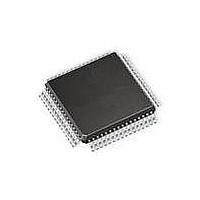
AT90CAN128-15AZ Atmel, AT90CAN128-15AZ Datasheet - Page 297

AT90CAN128-15AZ
Manufacturer Part Number
AT90CAN128-15AZ
Description
MCU AVR 128K FLASH 15MHZ 64TQFP
Manufacturer
Atmel
Series
AVR® 90CANr
Specifications of AT90CAN128-15AZ
Package / Case
64-TQFP, 64-VQFP
Voltage - Supply (vcc/vdd)
2.7 V ~ 5.5 V
Operating Temperature
-40°C ~ 125°C
Speed
16MHz
Number Of I /o
53
Eeprom Size
4K x 8
Core Processor
AVR
Program Memory Type
FLASH
Ram Size
4K x 8
Program Memory Size
128KB (128K x 8)
Data Converters
A/D 8x10b
Oscillator Type
Internal
Peripherals
Brown-out Detect/Reset, POR, PWM, WDT
Connectivity
CAN, I²C, SPI, UART/USART
Core Size
8-Bit
Processor Series
AT90CANx
Core
AVR8
Data Bus Width
8 bit
Data Ram Size
4 KB
Interface Type
CAN, SPI, UART
Maximum Clock Frequency
16 MHz
Number Of Programmable I/os
53
Number Of Timers
4
Maximum Operating Temperature
+ 125 C
Mounting Style
SMD/SMT
3rd Party Development Tools
EWAVR, EWAVR-BL
Development Tools By Supplier
ATAVRDRAGON, ATSTK500, ATSTK600, ATAVRISP2, ATDVK90CAN1, ATADAPCAN01
Minimum Operating Temperature
- 40 C
On-chip Adc
10 bit, 8 Channel
Cpu Family
90C
Device Core
AVR
Device Core Size
8b
Frequency (max)
16MHz
Total Internal Ram Size
4KB
# I/os (max)
53
Number Of Timers - General Purpose
4
Operating Supply Voltage (typ)
3.3/5V
Operating Supply Voltage (max)
5.5V
Operating Supply Voltage (min)
2.7V
Instruction Set Architecture
RISC
Operating Temp Range
-40C to 125C
Operating Temperature Classification
Automotive
Mounting
Surface Mount
Pin Count
64
Package Type
TQFP
Lead Free Status / RoHS Status
Lead free / RoHS Compliant
Available stocks
Company
Part Number
Manufacturer
Quantity
Price
Company:
Part Number:
AT90CAN128-15AZ
Manufacturer:
SAMSUNG
Quantity:
1 001
Company:
Part Number:
AT90CAN128-15AZ
Manufacturer:
ATMEL
Quantity:
1 000
Part Number:
AT90CAN128-15AZ
Manufacturer:
ATMEL/爱特梅尔
Quantity:
20 000
- Current page: 297 of 428
- Download datasheet (6Mb)
22.5
22.6
7679H–CAN–08/08
Using the Boundary-scan Chain
Using the On-chip Debug System
As shown in the state diagram, the Run-Test/Idle state need not be entered between selecting
JTAG instruction and using data registers, and some JTAG instructions may select certain func-
tions to be performed in the Run-Test/Idle, making it unsuitable as an Idle state.
Note:
For detailed information on the JTAG specification, refer to the literature listed in
on page
A complete description of the Boundary-scan capabilities are given in the section
scan IEEE 1149.1 (JTAG)” on page
As shown in
All read or modify/write operations needed for implementing the Debugger are done by applying
AVR instructions via the internal AVR CPU Scan Chain. The CPU sends the result to an I/O
memory mapped location which is part of the communication interface between the CPU and the
JTAG system.
The Break Point Unit implements Break on Change of Program Flow, Single Step Break, two
Program Memory Break Points, and two combined Break Points. Together, the four Break
Points can be configured as either:
• Apply the TMS sequence 1, 1, 0 to re-enter the Run-Test/Idle state. The instruction is latched
• At the TMS input, apply the sequence 1, 0, 0 at the rising edges of TCK to enter the Shift
• Apply the TMS sequence 1, 1, 0 to re-enter the Run-Test/Idle state. If the selected data
• A scan chain on the interface between the internal AVR CPU and the internal peripheral
• Break Point unit.
• Communication interface between the CPU and JTAG system.
• 4 single Program Memory Break Points.
• 3 single Program Memory Break Points + 1 single Data Memory Break Point.
• 2 single Program Memory Break Points + 2 single Data Memory Break Points.
onto the parallel output from the Shift Register path in the Update-IR state. The Exit-IR,
Pause-IR, and Exit2-IR states are only used for navigating the state machine.
Data Register – Shift-DR state. While in this state, upload the selected data register (selected
by the present JTAG instruction in the JTAG Instruction Register) from the TDI input at the
rising edge of TCK. In order to remain in the Shift-DR state, the TMS input must be held low
during input of all bits except the MSB. The MSB of the data is shifted in when this state is left
by setting TMS high. While the data register is shifted in from the TDI pin, the parallel inputs
to the data register captured in the Capture-DR state is shifted out on the TDO pin.
register has a latched parallel-output, the latching takes place in the Update-DR state. The
Exit-DR, Pause-DR, and Exit2-DR states are only used for navigating the state machine.
units.
Independent of the initial state of the TAP Controller, the Test-Logic-Reset state can always be
entered by holding TMS high for five TCK clock periods.
299.
Figure
22-1, the hardware support for On-chip Debugging consists mainly of
300.
AT90CAN32/64/128
“Bibliography”
“Boundary-
297
Related parts for AT90CAN128-15AZ
Image
Part Number
Description
Manufacturer
Datasheet
Request
R

Part Number:
Description:
DEV KIT FOR AVR/AVR32
Manufacturer:
Atmel
Datasheet:

Part Number:
Description:
INTERVAL AND WIPE/WASH WIPER CONTROL IC WITH DELAY
Manufacturer:
ATMEL Corporation
Datasheet:

Part Number:
Description:
Low-Voltage Voice-Switched IC for Hands-Free Operation
Manufacturer:
ATMEL Corporation
Datasheet:

Part Number:
Description:
MONOLITHIC INTEGRATED FEATUREPHONE CIRCUIT
Manufacturer:
ATMEL Corporation
Datasheet:

Part Number:
Description:
AM-FM Receiver IC U4255BM-M
Manufacturer:
ATMEL Corporation
Datasheet:

Part Number:
Description:
Monolithic Integrated Feature Phone Circuit
Manufacturer:
ATMEL Corporation
Datasheet:

Part Number:
Description:
Multistandard Video-IF and Quasi Parallel Sound Processing
Manufacturer:
ATMEL Corporation
Datasheet:

Part Number:
Description:
High-performance EE PLD
Manufacturer:
ATMEL Corporation
Datasheet:

Part Number:
Description:
8-bit Flash Microcontroller
Manufacturer:
ATMEL Corporation
Datasheet:

Part Number:
Description:
2-Wire Serial EEPROM
Manufacturer:
ATMEL Corporation
Datasheet:


