MC9S12C64CFUE Freescale Semiconductor, MC9S12C64CFUE Datasheet - Page 201
MC9S12C64CFUE
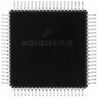
Manufacturer Part Number
MC9S12C64CFUE
Description
IC MCU 64K FLASH 4K RAM 80-QFP
Manufacturer
Freescale Semiconductor
Series
HCS12r
Specifications of MC9S12C64CFUE
Core Processor
HCS12
Core Size
16-Bit
Speed
25MHz
Connectivity
CAN, EBI/EMI, SCI, SPI
Peripherals
POR, PWM, WDT
Number Of I /o
60
Program Memory Size
64KB (64K x 8)
Program Memory Type
FLASH
Ram Size
4K x 8
Voltage - Supply (vcc/vdd)
2.35 V ~ 5.5 V
Data Converters
A/D 8x10b
Oscillator Type
Internal
Operating Temperature
-40°C ~ 85°C
Package / Case
80-QFP
Processor Series
S12C
Core
HCS12
Data Bus Width
16 bit
Data Ram Size
4 KB
Interface Type
CAN/SCI/SPI
Maximum Clock Frequency
25 MHz
Number Of Programmable I/os
60
Number Of Timers
8
Maximum Operating Temperature
+ 85 C
Mounting Style
SMD/SMT
3rd Party Development Tools
EWHCS12
Development Tools By Supplier
M68EVB912C32EE
Minimum Operating Temperature
- 40 C
On-chip Adc
8-ch x 10-bit
Package
80PQFP
Family Name
HCS12
Maximum Speed
25 MHz
Operating Supply Voltage
2.5|5 V
Height
2.4 mm
Length
14 mm
Supply Voltage (max)
2.75 V, 5.5 V
Supply Voltage (min)
2.35 V, 2.97 V
Width
14 mm
Lead Free Status / RoHS Status
Lead free / RoHS Compliant
Eeprom Size
-
Lead Free Status / Rohs Status
Lead free / RoHS Compliant
Available stocks
Company
Part Number
Manufacturer
Quantity
Price

Company:
Part Number:
MC9S12C64CFUE
Manufacturer:
Freescale Semiconductor
Quantity:
10 000


7.3.2.3
Freescale Semiconductor
Module Base + 0x0022
Starting address location affected by INITRG register setting.
Module Base + 0x0023
Starting address location affected by INITRG register setting.
Reset
Reset
Field
15:0
W
W
R
R
Bit 15
Bit 7
Trace Buffer Data Bits — The trace buffer data bits contain the data of the trace buffer. This register can be read
only as a word read. Any byte reads or misaligned access of these registers will return 0 and will not cause the
trace buffer pointer to increment to the next trace buffer address. The same is true for word reads while the
debugger is armed. In addition, this register may appear to contain incorrect data if it is not read with the same
capture mode bit settings as when the trace buffer data was recorded (See
Trace
Debug Trace Buffer Register (DBGTB)
15
u
u
7
Buffer”). Because reads will reflect the contents of the trace buffer RAM, the reset state is undefined.
= Unimplemented or Reserved
= Unimplemented or Reserved
Bit 14
Bit 6
Figure 7-6. Debug Trace Buffer Register High (DBGTBH)
Figure 7-7. Debug Trace Buffer Register Low (DBGTBL)
14
u
u
6
Table 7-7. DBGTB Field Descriptions
Bit 13
MC9S12C-Family / MC9S12GC-Family
Bit 5
13
u
u
5
Bit 12
Rev 01.24
Bit 4
12
u
u
4
Description
Bit 11
Bit 3
11
u
u
3
Chapter 7 Debug Module (DBGV1) Block Description
Bit 10
Bit 2
10
u
u
Section 7.4.2.9, “Reading Data from
2
Bit 9
Bit 1
u
u
9
1
Bit 8
Bit 0
u
u
8
0
201
Related parts for MC9S12C64CFUE
Image
Part Number
Description
Manufacturer
Datasheet
Request
R

Part Number:
Description:
Manufacturer:
Freescale Semiconductor, Inc
Datasheet:
Part Number:
Description:
Manufacturer:
Freescale Semiconductor, Inc
Datasheet:
Part Number:
Description:
Manufacturer:
Freescale Semiconductor, Inc
Datasheet:
Part Number:
Description:
Manufacturer:
Freescale Semiconductor, Inc
Datasheet:
Part Number:
Description:
Manufacturer:
Freescale Semiconductor, Inc
Datasheet:
Part Number:
Description:
Manufacturer:
Freescale Semiconductor, Inc
Datasheet:
Part Number:
Description:
Manufacturer:
Freescale Semiconductor, Inc
Datasheet:
Part Number:
Description:
Manufacturer:
Freescale Semiconductor, Inc
Datasheet:
Part Number:
Description:
Manufacturer:
Freescale Semiconductor, Inc
Datasheet:
Part Number:
Description:
Manufacturer:
Freescale Semiconductor, Inc
Datasheet:
Part Number:
Description:
Manufacturer:
Freescale Semiconductor, Inc
Datasheet:
Part Number:
Description:
Manufacturer:
Freescale Semiconductor, Inc
Datasheet:
Part Number:
Description:
Manufacturer:
Freescale Semiconductor, Inc
Datasheet:
Part Number:
Description:
Manufacturer:
Freescale Semiconductor, Inc
Datasheet:
Part Number:
Description:
Manufacturer:
Freescale Semiconductor, Inc
Datasheet: