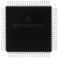
MC9S12C64CFUE Freescale Semiconductor, MC9S12C64CFUE Datasheet - Page 322

MC9S12C64CFUE
Manufacturer Part Number
MC9S12C64CFUE
Description
IC MCU 64K FLASH 4K RAM 80-QFP
Manufacturer
Freescale Semiconductor
Series
HCS12r
Specifications of MC9S12C64CFUE
Core Processor
HCS12
Core Size
16-Bit
Speed
25MHz
Connectivity
CAN, EBI/EMI, SCI, SPI
Peripherals
POR, PWM, WDT
Number Of I /o
60
Program Memory Size
64KB (64K x 8)
Program Memory Type
FLASH
Ram Size
4K x 8
Voltage - Supply (vcc/vdd)
2.35 V ~ 5.5 V
Data Converters
A/D 8x10b
Oscillator Type
Internal
Operating Temperature
-40°C ~ 85°C
Package / Case
80-QFP
Processor Series
S12C
Core
HCS12
Data Bus Width
16 bit
Data Ram Size
4 KB
Interface Type
CAN/SCI/SPI
Maximum Clock Frequency
25 MHz
Number Of Programmable I/os
60
Number Of Timers
8
Maximum Operating Temperature
+ 85 C
Mounting Style
SMD/SMT
3rd Party Development Tools
EWHCS12
Development Tools By Supplier
M68EVB912C32EE
Minimum Operating Temperature
- 40 C
On-chip Adc
8-ch x 10-bit
Package
80PQFP
Family Name
HCS12
Maximum Speed
25 MHz
Operating Supply Voltage
2.5|5 V
Height
2.4 mm
Length
14 mm
Supply Voltage (max)
2.75 V, 5.5 V
Supply Voltage (min)
2.35 V, 2.97 V
Width
14 mm
Lead Free Status / RoHS Status
Lead free / RoHS Compliant
Eeprom Size
-
Lead Free Status / Rohs Status
Lead free / RoHS Compliant
Available stocks
Company
Part Number
Manufacturer
Quantity
Price
Company:
Part Number:
MC9S12C64CFUE
Manufacturer:
Freescale Semiconductor
Quantity:
10 000
- Current page: 322 of 690
- Download datasheet (4Mb)
Chapter 10 Freescale’s Scalable Controller Area Network (S12MSCANV2)
In cases of more than one buffer having the same lowest priority, the message buffer with the lower index
number wins.
Read: Anytime when TXEx flag is set (see
(CANTFLG)”) and the corresponding transmit buffer is selected in CANTBSEL (see
“MSCAN Transmit Buffer Selection Register
Write: Anytime when TXEx flag is set (see
(CANTFLG)”) and the corresponding transmit buffer is selected in CANTBSEL (see
“MSCAN Transmit Buffer Selection Register
10.3.3.5
If the TIME bit is enabled, the MSCAN will write a time stamp to the respective registers in the active
transmit or receive buffer right after the EOF of a valid message on the CAN bus (see
“MSCAN Control Register 0
stamp after the respective transmit buffer has been flagged empty.
The timer value, which is used for stamping, is taken from a free running internal CAN bit clock. A timer
overrun is not indicated by the MSCAN. The timer is reset (all bits set to 0) during initialization mode. The
CPU can only read the time stamp registers.
322
Module Base + 0xXXXD
Module Base + 0xXXXE
Module Base + 0xXXXF
Reset:
Reset:
Reset:
W
W
W
R
R
R
Time Stamp Register (TSRH–TSRL)
TSR15
PRIO7
TSR7
0
7
7
x
7
x
Figure 10-36. Time Stamp Register — High Byte (TSRH)
Figure 10-37. Time Stamp Register — Low Byte (TSRL)
Figure 10-35. Transmit Buffer Priority Register (TBPR)
TSR14
PRIO6
TSR6
6
0
6
x
6
x
(CANCTL0)”). In case of a transmission, the CPU can only read the time
MC9S12C-Family / MC9S12GC-Family
TSR13
PRIO5
TSR5
0
5
5
x
5
x
Section 10.3.2.7, “MSCAN Transmitter Flag Register
Section 10.3.2.7, “MSCAN Transmitter Flag Register
(CANTBSEL)”).
(CANTBSEL)”).
Rev 01.24
TSR12
PRIO4
TSR4
4
0
4
x
4
x
TSR11
PRIO3
TSR3
0
x
x
3
3
3
TSR10
PRIO2
TSR2
2
0
2
x
2
x
Freescale Semiconductor
PRIO1
TSR9
TSR1
Section 10.3.2.11,
Section 10.3.2.11,
Section 10.3.2.1,
0
x
x
1
1
1
PRIO0
TSR8
TSR0
0
0
0
x
0
x
Related parts for MC9S12C64CFUE
Image
Part Number
Description
Manufacturer
Datasheet
Request
R
Part Number:
Description:
Manufacturer:
Freescale Semiconductor, Inc
Datasheet:
Part Number:
Description:
Manufacturer:
Freescale Semiconductor, Inc
Datasheet:
Part Number:
Description:
Manufacturer:
Freescale Semiconductor, Inc
Datasheet:
Part Number:
Description:
Manufacturer:
Freescale Semiconductor, Inc
Datasheet:
Part Number:
Description:
Manufacturer:
Freescale Semiconductor, Inc
Datasheet:
Part Number:
Description:
Manufacturer:
Freescale Semiconductor, Inc
Datasheet:
Part Number:
Description:
Manufacturer:
Freescale Semiconductor, Inc
Datasheet:
Part Number:
Description:
Manufacturer:
Freescale Semiconductor, Inc
Datasheet:
Part Number:
Description:
Manufacturer:
Freescale Semiconductor, Inc
Datasheet:
Part Number:
Description:
Manufacturer:
Freescale Semiconductor, Inc
Datasheet:
Part Number:
Description:
Manufacturer:
Freescale Semiconductor, Inc
Datasheet:
Part Number:
Description:
Manufacturer:
Freescale Semiconductor, Inc
Datasheet:
Part Number:
Description:
Manufacturer:
Freescale Semiconductor, Inc
Datasheet:
Part Number:
Description:
Manufacturer:
Freescale Semiconductor, Inc
Datasheet:
Part Number:
Description:
Manufacturer:
Freescale Semiconductor, Inc
Datasheet:


