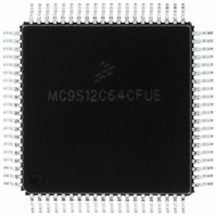
MC9S12C64CFUE Freescale Semiconductor, MC9S12C64CFUE Datasheet - Page 283

MC9S12C64CFUE
Manufacturer Part Number
MC9S12C64CFUE
Description
IC MCU 64K FLASH 4K RAM 80-QFP
Manufacturer
Freescale Semiconductor
Series
HCS12r
Specifications of MC9S12C64CFUE
Core Processor
HCS12
Core Size
16-Bit
Speed
25MHz
Connectivity
CAN, EBI/EMI, SCI, SPI
Peripherals
POR, PWM, WDT
Number Of I /o
60
Program Memory Size
64KB (64K x 8)
Program Memory Type
FLASH
Ram Size
4K x 8
Voltage - Supply (vcc/vdd)
2.35 V ~ 5.5 V
Data Converters
A/D 8x10b
Oscillator Type
Internal
Operating Temperature
-40°C ~ 85°C
Package / Case
80-QFP
Processor Series
S12C
Core
HCS12
Data Bus Width
16 bit
Data Ram Size
4 KB
Interface Type
CAN/SCI/SPI
Maximum Clock Frequency
25 MHz
Number Of Programmable I/os
60
Number Of Timers
8
Maximum Operating Temperature
+ 85 C
Mounting Style
SMD/SMT
3rd Party Development Tools
EWHCS12
Development Tools By Supplier
M68EVB912C32EE
Minimum Operating Temperature
- 40 C
On-chip Adc
8-ch x 10-bit
Package
80PQFP
Family Name
HCS12
Maximum Speed
25 MHz
Operating Supply Voltage
2.5|5 V
Height
2.4 mm
Length
14 mm
Supply Voltage (max)
2.75 V, 5.5 V
Supply Voltage (min)
2.35 V, 2.97 V
Width
14 mm
Lead Free Status / RoHS Status
Lead free / RoHS Compliant
Eeprom Size
-
Lead Free Status / Rohs Status
Lead free / RoHS Compliant
Available stocks
Company
Part Number
Manufacturer
Quantity
Price
Company:
Part Number:
MC9S12C64CFUE
Manufacturer:
Freescale Semiconductor
Quantity:
10 000
- Current page: 283 of 690
- Download datasheet (4Mb)
Definition.” All reset sources are listed in
vector addresses and priorities.
The reset sequence is initiated by any of the following events:
Upon detection of any reset event, an internal circuit drives the RESET pin low for 128 SYSCLK cycles
(see
However, the internal reset circuit of the CRGV4 cannot sequence out of current reset condition without a
running SYSCLK. The number of 128 SYSCLK cycles might be increased by n = 3 to 6 additional
SYSCLK cycles depending on the internal synchronization latency. After 128+n SYSCLK cycles the
RESET pin is released. The reset generator of the CRGV4 waits for additional 64 SYSCLK cycles and
then samples the RESET pin to determine the originating source.
fetched.
Freescale Semiconductor
•
•
•
•
•
Figure
Low level is detected at the RESET pin (external reset).
Power on is detected.
Low voltage is detected.
COP watchdog times out.
Clock monitor failure is detected and self-clock mode was disabled (SCME = 0).
9-25). Because entry into reset is asynchronous it does not require a running SYSCLK.
External circuitry connected to the RESET pin should not include a large
capacitance that would interfere with the ability of this signal to rise to a
valid logic 1 within 64 SYSCLK cycles after the low drive is released.
Sampled RESET Pin
(64 Cycles After
Release)
1
1
1
0
COP Watchdog Reset
Clock Monitor Reset
Low Voltage Reset
Power-on Reset
External Reset
Reset Source
Table 9-14. Reset Vector Selection
MC9S12C-Family / MC9S12GC-Family
Reset Pending
Clock Monitor
Table 9-13. Reset Summary
Table
X
0
1
0
9-13. Refer to the device overview chapter for related
Rev 01.24
NOTE
PLLCTL (CME=1, SCME=0)
COPCTL (CR[2:0] nonzero)
Chapter 9 Clocks and Reset Generator (CRGV4) Block Description
COP Reset
Pending
Local Enable
X
X
0
1
None
None
None
POR / LVR / External Reset
Clock Monitor Reset
COP Reset
POR / LVR / External Reset
with rise of RESET pin
Table 9-14
Vector Fetch
shows which vector will be
283
Related parts for MC9S12C64CFUE
Image
Part Number
Description
Manufacturer
Datasheet
Request
R
Part Number:
Description:
Manufacturer:
Freescale Semiconductor, Inc
Datasheet:
Part Number:
Description:
Manufacturer:
Freescale Semiconductor, Inc
Datasheet:
Part Number:
Description:
Manufacturer:
Freescale Semiconductor, Inc
Datasheet:
Part Number:
Description:
Manufacturer:
Freescale Semiconductor, Inc
Datasheet:
Part Number:
Description:
Manufacturer:
Freescale Semiconductor, Inc
Datasheet:
Part Number:
Description:
Manufacturer:
Freescale Semiconductor, Inc
Datasheet:
Part Number:
Description:
Manufacturer:
Freescale Semiconductor, Inc
Datasheet:
Part Number:
Description:
Manufacturer:
Freescale Semiconductor, Inc
Datasheet:
Part Number:
Description:
Manufacturer:
Freescale Semiconductor, Inc
Datasheet:
Part Number:
Description:
Manufacturer:
Freescale Semiconductor, Inc
Datasheet:
Part Number:
Description:
Manufacturer:
Freescale Semiconductor, Inc
Datasheet:
Part Number:
Description:
Manufacturer:
Freescale Semiconductor, Inc
Datasheet:
Part Number:
Description:
Manufacturer:
Freescale Semiconductor, Inc
Datasheet:
Part Number:
Description:
Manufacturer:
Freescale Semiconductor, Inc
Datasheet:
Part Number:
Description:
Manufacturer:
Freescale Semiconductor, Inc
Datasheet:


