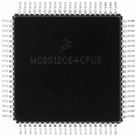
MC9S12C64CFUE Freescale Semiconductor, MC9S12C64CFUE Datasheet - Page 349

MC9S12C64CFUE
Manufacturer Part Number
MC9S12C64CFUE
Description
IC MCU 64K FLASH 4K RAM 80-QFP
Manufacturer
Freescale Semiconductor
Series
HCS12r
Specifications of MC9S12C64CFUE
Core Processor
HCS12
Core Size
16-Bit
Speed
25MHz
Connectivity
CAN, EBI/EMI, SCI, SPI
Peripherals
POR, PWM, WDT
Number Of I /o
60
Program Memory Size
64KB (64K x 8)
Program Memory Type
FLASH
Ram Size
4K x 8
Voltage - Supply (vcc/vdd)
2.35 V ~ 5.5 V
Data Converters
A/D 8x10b
Oscillator Type
Internal
Operating Temperature
-40°C ~ 85°C
Package / Case
80-QFP
Processor Series
S12C
Core
HCS12
Data Bus Width
16 bit
Data Ram Size
4 KB
Interface Type
CAN/SCI/SPI
Maximum Clock Frequency
25 MHz
Number Of Programmable I/os
60
Number Of Timers
8
Maximum Operating Temperature
+ 85 C
Mounting Style
SMD/SMT
3rd Party Development Tools
EWHCS12
Development Tools By Supplier
M68EVB912C32EE
Minimum Operating Temperature
- 40 C
On-chip Adc
8-ch x 10-bit
Package
80PQFP
Family Name
HCS12
Maximum Speed
25 MHz
Operating Supply Voltage
2.5|5 V
Height
2.4 mm
Length
14 mm
Supply Voltage (max)
2.75 V, 5.5 V
Supply Voltage (min)
2.35 V, 2.97 V
Width
14 mm
Lead Free Status / RoHS Status
Lead free / RoHS Compliant
Eeprom Size
-
Lead Free Status / Rohs Status
Lead free / RoHS Compliant
Available stocks
Company
Part Number
Manufacturer
Quantity
Price
Company:
Part Number:
MC9S12C64CFUE
Manufacturer:
Freescale Semiconductor
Quantity:
10 000
- Current page: 349 of 690
- Download datasheet (4Mb)
12.2.4
This pin serves as waveform output of PWM channel 2.
12.2.5
This pin serves as waveform output of PWM channel 1.
12.2.6
This pin serves as waveform output of PWM channel 0.
12.3
This subsection describes in detail all the registers and register bits in the PWM8B6CV1 module.
The special-purpose registers and register bit functions that would not normally be made available to
device end users, such as factory test control registers and reserved registers are clearly identified by means
of shading the appropriate portions of address maps and register diagrams. Notes explaining the reasons
for restricting access to the registers and functions are also explained in the individual register descriptions.
12.3.1
The following paragraphs describe the content of the registers in the PWM8B6CV1 module. The base
address of the PWM8B6CV1 module is determined at the MCU level when the MCU is defined. The
register decode map is fixed and begins at the first address of the module address offset.
the registers associated with the PWM and their relative offset from the base address. The register detail
description follows the order in which they appear in the register map.
Reserved bits within a register will always read as 0 and the write will be unimplemented. Unimplemented
functions are indicated by shading the bit.
Table 12-1
Freescale Semiconductor
Memory Map and Register Definition
shows the memory map for the PWM8B6CV1 module.
PWM2 — Pulse Width Modulator Channel 2 Pin
PWM1 — Pulse Width Modulator Channel 1 Pin
PWM0 — Pulse Width Modulator Channel 0 Pin
Module Memory Map
Register address = base address + address offset, where the base address is
defined at the MCU level and the address offset is defined at the module
level.
MC9S12C-Family / MC9S12GC-Family
Rev 01.24
NOTE
Chapter 12 Pulse-Width Modulator (PWM8B6CV1) Block Description
Table 12-1
shows
349
Related parts for MC9S12C64CFUE
Image
Part Number
Description
Manufacturer
Datasheet
Request
R
Part Number:
Description:
Manufacturer:
Freescale Semiconductor, Inc
Datasheet:
Part Number:
Description:
Manufacturer:
Freescale Semiconductor, Inc
Datasheet:
Part Number:
Description:
Manufacturer:
Freescale Semiconductor, Inc
Datasheet:
Part Number:
Description:
Manufacturer:
Freescale Semiconductor, Inc
Datasheet:
Part Number:
Description:
Manufacturer:
Freescale Semiconductor, Inc
Datasheet:
Part Number:
Description:
Manufacturer:
Freescale Semiconductor, Inc
Datasheet:
Part Number:
Description:
Manufacturer:
Freescale Semiconductor, Inc
Datasheet:
Part Number:
Description:
Manufacturer:
Freescale Semiconductor, Inc
Datasheet:
Part Number:
Description:
Manufacturer:
Freescale Semiconductor, Inc
Datasheet:
Part Number:
Description:
Manufacturer:
Freescale Semiconductor, Inc
Datasheet:
Part Number:
Description:
Manufacturer:
Freescale Semiconductor, Inc
Datasheet:
Part Number:
Description:
Manufacturer:
Freescale Semiconductor, Inc
Datasheet:
Part Number:
Description:
Manufacturer:
Freescale Semiconductor, Inc
Datasheet:
Part Number:
Description:
Manufacturer:
Freescale Semiconductor, Inc
Datasheet:
Part Number:
Description:
Manufacturer:
Freescale Semiconductor, Inc
Datasheet:


