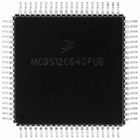
MC9S12C64CFUE Freescale Semiconductor, MC9S12C64CFUE Datasheet - Page 243

MC9S12C64CFUE
Manufacturer Part Number
MC9S12C64CFUE
Description
IC MCU 64K FLASH 4K RAM 80-QFP
Manufacturer
Freescale Semiconductor
Series
HCS12r
Specifications of MC9S12C64CFUE
Core Processor
HCS12
Core Size
16-Bit
Speed
25MHz
Connectivity
CAN, EBI/EMI, SCI, SPI
Peripherals
POR, PWM, WDT
Number Of I /o
60
Program Memory Size
64KB (64K x 8)
Program Memory Type
FLASH
Ram Size
4K x 8
Voltage - Supply (vcc/vdd)
2.35 V ~ 5.5 V
Data Converters
A/D 8x10b
Oscillator Type
Internal
Operating Temperature
-40°C ~ 85°C
Package / Case
80-QFP
Processor Series
S12C
Core
HCS12
Data Bus Width
16 bit
Data Ram Size
4 KB
Interface Type
CAN/SCI/SPI
Maximum Clock Frequency
25 MHz
Number Of Programmable I/os
60
Number Of Timers
8
Maximum Operating Temperature
+ 85 C
Mounting Style
SMD/SMT
3rd Party Development Tools
EWHCS12
Development Tools By Supplier
M68EVB912C32EE
Minimum Operating Temperature
- 40 C
On-chip Adc
8-ch x 10-bit
Package
80PQFP
Family Name
HCS12
Maximum Speed
25 MHz
Operating Supply Voltage
2.5|5 V
Height
2.4 mm
Length
14 mm
Supply Voltage (max)
2.75 V, 5.5 V
Supply Voltage (min)
2.35 V, 2.97 V
Width
14 mm
Lead Free Status / RoHS Status
Lead free / RoHS Compliant
Eeprom Size
-
Lead Free Status / Rohs Status
Lead free / RoHS Compliant
Available stocks
Company
Part Number
Manufacturer
Quantity
Price
Company:
Part Number:
MC9S12C64CFUE
Manufacturer:
Freescale Semiconductor
Quantity:
10 000
- Current page: 243 of 690
- Download datasheet (4Mb)
8.3.2.12
The data port associated with the ATD is general purpose I/O. The port pins are shared with the analog
A/D inputs AN7–AN0.
Read: Anytime
Write: Anytime, no effect
The A/D input channels may be used for general-purpose digital I/0.
8.3.2.13
The A/D conversion results are stored in 8 read-only result registers ATDDRHx/ATDDRLx. The result
data is formatted in the result registers based on two criteria. First there is left and right justification; this
selection is made using the DJM control bit in ATDCTL5. Second there is signed and unsigned data; this
selection is made using the DSGN control bit in ATDCTL5. Signed data is stored in 2’s complement
format and only exists in left justified format. Signed data selected for right justified format is ignored.
Read: Anytime
Write: Anytime, no effect in normal modes
Freescale Semiconductor
Function
Module Base + 0x000F
PTAD[7:0]
Reset
Field
Pin
7
W
R
PTAD7
AN7
A/D Channel x (ANx) Digital Input (x = 7, 6, 5, 4, 3, 2, 1, 0) — If the digital input buffer on the ANx pin is enabled
(IENx = 1) read returns the logic level on ANx pin (signal potentials not meeting V
an indeterminate value)).
If the digital input buffers are disabled (IENx = 0), read returns a “1”.
Reset sets all PORTAD bits to “1”.
Port Data Register (PORTAD)
ATD Conversion Result Registers (ATDDRHx/ATDDRLx)
1
7
= Unimplemented or Reserved
PTAD6
AN6
1
6
Figure 8-14. Port Data Register (PORTAD)
Table 8-18. PORTAD Field Descriptions
PTAD5
MC9S12C-Family / MC9S12GC-Family
AN5
1
5
PTAD4
Rev 01.24
AN4
1
4
Chapter 8 Analog-to-Digital Converter (ATD10B8C) Block Description
Description
PTAD3
AN3‘
1
3
PTAD2
AN2
1
2
IL
or V
IH
PTAD1
AN1
specifications will have
1
1
PTAD0
AN0
1
0
243
Related parts for MC9S12C64CFUE
Image
Part Number
Description
Manufacturer
Datasheet
Request
R
Part Number:
Description:
Manufacturer:
Freescale Semiconductor, Inc
Datasheet:
Part Number:
Description:
Manufacturer:
Freescale Semiconductor, Inc
Datasheet:
Part Number:
Description:
Manufacturer:
Freescale Semiconductor, Inc
Datasheet:
Part Number:
Description:
Manufacturer:
Freescale Semiconductor, Inc
Datasheet:
Part Number:
Description:
Manufacturer:
Freescale Semiconductor, Inc
Datasheet:
Part Number:
Description:
Manufacturer:
Freescale Semiconductor, Inc
Datasheet:
Part Number:
Description:
Manufacturer:
Freescale Semiconductor, Inc
Datasheet:
Part Number:
Description:
Manufacturer:
Freescale Semiconductor, Inc
Datasheet:
Part Number:
Description:
Manufacturer:
Freescale Semiconductor, Inc
Datasheet:
Part Number:
Description:
Manufacturer:
Freescale Semiconductor, Inc
Datasheet:
Part Number:
Description:
Manufacturer:
Freescale Semiconductor, Inc
Datasheet:
Part Number:
Description:
Manufacturer:
Freescale Semiconductor, Inc
Datasheet:
Part Number:
Description:
Manufacturer:
Freescale Semiconductor, Inc
Datasheet:
Part Number:
Description:
Manufacturer:
Freescale Semiconductor, Inc
Datasheet:
Part Number:
Description:
Manufacturer:
Freescale Semiconductor, Inc
Datasheet:


