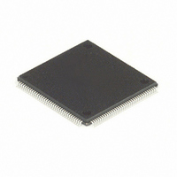
MC68HC16Z1CAG25 Freescale Semiconductor, MC68HC16Z1CAG25 Datasheet - Page 169

MC68HC16Z1CAG25
Manufacturer Part Number
MC68HC16Z1CAG25
Description
IC MCU 16BIT 25MHZ 144-LQFP
Manufacturer
Freescale Semiconductor
Series
HC16r
Datasheet
1.MC68HC16Z1VEH16.pdf
(500 pages)
Specifications of MC68HC16Z1CAG25
Core Processor
CPU16
Core Size
16-Bit
Speed
25MHz
Connectivity
EBI/EMI, SCI, SPI
Peripherals
POR, PWM, WDT
Number Of I /o
16
Program Memory Type
ROMless
Ram Size
1K x 8
Voltage - Supply (vcc/vdd)
2.7 V ~ 5.5 V
Data Converters
A/D 8x10b
Oscillator Type
Internal
Operating Temperature
-40°C ~ 85°C
Package / Case
144-LQFP
Cpu Family
HC16
Device Core Size
16b
Frequency (max)
25MHz
Interface Type
SCI/SPI/UART
Program Memory Size
Not Required
Total Internal Ram Size
1KB
# I/os (max)
16
Number Of Timers - General Purpose
11
Operating Supply Voltage (typ)
3.3/5V
Operating Supply Voltage (max)
5.5V
Operating Supply Voltage (min)
2.7V
On-chip Adc
8-chx10-bit
Instruction Set Architecture
CISC
Operating Temp Range
-40C to 85C
Operating Temperature Classification
Industrial
Mounting
Surface Mount
Pin Count
144
Package Type
LQFP
Controller Family/series
68HC16
No. Of I/o's
16
Ram Memory Size
1KB
Cpu Speed
25MHz
No. Of Timers
2
Embedded Interface Type
QSPI, SCI
Rohs Compliant
Yes
Processor Series
HC16Z
Core
CPU16
Data Bus Width
16 bit
Data Ram Size
1 KB
Maximum Clock Frequency
25 MHz
Number Of Programmable I/os
16
Number Of Timers
11
Maximum Operating Temperature
+ 85 C
Mounting Style
SMD/SMT
Minimum Operating Temperature
- 40 C
Lead Free Status / RoHS Status
Lead free / RoHS Compliant
Eeprom Size
-
Program Memory Size
-
Lead Free Status / Rohs Status
Compliant
Available stocks
Company
Part Number
Manufacturer
Quantity
Price
Company:
Part Number:
MC68HC16Z1CAG25
Manufacturer:
FREESCAL
Quantity:
455
Company:
Part Number:
MC68HC16Z1CAG25
Manufacturer:
Freescale Semiconductor
Quantity:
10 000
- Current page: 169 of 500
- Download datasheet (6Mb)
5.9.1 Chip-Select Registers
M68HC16 Z SERIES
USER’S MANUAL
Chip-select assertion can be synchronized with bus control signals to provide output
enable, read/write strobe, or interrupt acknowledge signals. Logic can also generate
DSACK and AVEC signals internally. A single DSACK generator is shared by all chip-
selects. Each signal can also be synchronized with the ECLK signal available on
ADDR23.
When a memory access occurs, chip-select logic compares address space type, ad-
dress, type of access, transfer size, and interrupt priority (in the case of interrupt ac-
knowledge) to parameters stored in chip-select registers. If all parameters match, the
appropriate chip-select signal is asserted. Select signals are active low. If a chip-select
function is given the same address as a microcontroller module or an internal memory
array, an access to that address goes to the module or array, and the chip-select sig-
nal is not asserted. The external address and data buses do not reflect the internal ac-
cess.
All chip-select circuits are configured for operation out of reset. However, all chip-se-
lect signals except CSBOOT are disabled, and cannot be asserted until the BYTE[1:0]
field in the corresponding option register is programmed to a non-zero value to select
a transfer size. The chip-select option register must not be written until a base address
has been written to a proper base address register. Alternate functions for chip-select
pins are enabled if appropriate data bus pins are held low at the release of RESET.
Refer to
functional diagram of a single chip-select circuit.
Each chip-select pin can have one or more functions. Chip-select pin assignment reg-
isters CSPAR[1:0] determine functions of the pins. Pin assignment registers also de-
termine port size (8- or 16-bit) for dynamic bus allocation. A pin data register (PORTC)
latches data for chip-select pins that are used for discrete output.
DSACK
BUS CONTROL
AVEC
5.7.3.1 Data Bus Mode Selection
ADDRESS
INTERNAL
SIGNALS
Figure 5-22 Chip-Select Circuit Block Diagram
Freescale Semiconductor, Inc.
GENERATOR
For More Information On This Product,
AVEC
BASE ADDRESS REGISTER
ADDRESS COMPARATOR
SYSTEM INTEGRATION MODULE
OPTION COMPARE
OPTION REGISTER
Go to: www.freescale.com
GENERATOR
DSACK
for more information.
ASSIGNMENT
REGISTER
PIN
CONTROL
TIMING
AND
REGISTER
DATA
PIN
Figure 5-22
PIN
CHIP SEL BLOCK
is a
5-63
Related parts for MC68HC16Z1CAG25
Image
Part Number
Description
Manufacturer
Datasheet
Request
R
Part Number:
Description:
Manufacturer:
Freescale Semiconductor, Inc
Datasheet:
Part Number:
Description:
Manufacturer:
Freescale Semiconductor, Inc
Datasheet:
Part Number:
Description:
Manufacturer:
Freescale Semiconductor, Inc
Datasheet:
Part Number:
Description:
Manufacturer:
Freescale Semiconductor, Inc
Datasheet:
Part Number:
Description:
Manufacturer:
Freescale Semiconductor, Inc
Datasheet:
Part Number:
Description:
Manufacturer:
Freescale Semiconductor, Inc
Datasheet:
Part Number:
Description:
Manufacturer:
Freescale Semiconductor, Inc
Datasheet:
Part Number:
Description:
Manufacturer:
Freescale Semiconductor, Inc
Datasheet:
Part Number:
Description:
Manufacturer:
Freescale Semiconductor, Inc
Datasheet:
Part Number:
Description:
Manufacturer:
Freescale Semiconductor, Inc
Datasheet:
Part Number:
Description:
Manufacturer:
Freescale Semiconductor, Inc
Datasheet:
Part Number:
Description:
Manufacturer:
Freescale Semiconductor, Inc
Datasheet:
Part Number:
Description:
Manufacturer:
Freescale Semiconductor, Inc
Datasheet:
Part Number:
Description:
Manufacturer:
Freescale Semiconductor, Inc
Datasheet:
Part Number:
Description:
Manufacturer:
Freescale Semiconductor, Inc
Datasheet:


