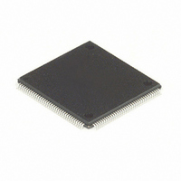
MC68HC16Z1CAG25 Freescale Semiconductor, MC68HC16Z1CAG25 Datasheet - Page 212

MC68HC16Z1CAG25
Manufacturer Part Number
MC68HC16Z1CAG25
Description
IC MCU 16BIT 25MHZ 144-LQFP
Manufacturer
Freescale Semiconductor
Series
HC16r
Datasheet
1.MC68HC16Z1VEH16.pdf
(500 pages)
Specifications of MC68HC16Z1CAG25
Core Processor
CPU16
Core Size
16-Bit
Speed
25MHz
Connectivity
EBI/EMI, SCI, SPI
Peripherals
POR, PWM, WDT
Number Of I /o
16
Program Memory Type
ROMless
Ram Size
1K x 8
Voltage - Supply (vcc/vdd)
2.7 V ~ 5.5 V
Data Converters
A/D 8x10b
Oscillator Type
Internal
Operating Temperature
-40°C ~ 85°C
Package / Case
144-LQFP
Cpu Family
HC16
Device Core Size
16b
Frequency (max)
25MHz
Interface Type
SCI/SPI/UART
Program Memory Size
Not Required
Total Internal Ram Size
1KB
# I/os (max)
16
Number Of Timers - General Purpose
11
Operating Supply Voltage (typ)
3.3/5V
Operating Supply Voltage (max)
5.5V
Operating Supply Voltage (min)
2.7V
On-chip Adc
8-chx10-bit
Instruction Set Architecture
CISC
Operating Temp Range
-40C to 85C
Operating Temperature Classification
Industrial
Mounting
Surface Mount
Pin Count
144
Package Type
LQFP
Controller Family/series
68HC16
No. Of I/o's
16
Ram Memory Size
1KB
Cpu Speed
25MHz
No. Of Timers
2
Embedded Interface Type
QSPI, SCI
Rohs Compliant
Yes
Processor Series
HC16Z
Core
CPU16
Data Bus Width
16 bit
Data Ram Size
1 KB
Maximum Clock Frequency
25 MHz
Number Of Programmable I/os
16
Number Of Timers
11
Maximum Operating Temperature
+ 85 C
Mounting Style
SMD/SMT
Minimum Operating Temperature
- 40 C
Lead Free Status / RoHS Status
Lead free / RoHS Compliant
Eeprom Size
-
Program Memory Size
-
Lead Free Status / Rohs Status
Compliant
Available stocks
Company
Part Number
Manufacturer
Quantity
Price
Company:
Part Number:
MC68HC16Z1CAG25
Manufacturer:
FREESCAL
Quantity:
455
Company:
Part Number:
MC68HC16Z1CAG25
Manufacturer:
Freescale Semiconductor
Quantity:
10 000
- Current page: 212 of 500
- Download datasheet (6Mb)
9.2 QSM Registers and Address Map
9.2.1 QSM Global Registers
9.2.1.1 Low-Power Stop Mode Operation
9-2
The SCI provides a standard non-return to zero (NRZ) mark/space format. It operates
in either full- or half-duplex mode. There are separate transmitter and receiver enable
bits and dual data buffers. A modulus-type baud rate generator provides rates from
110 baud to 781 kbaud with a 25.17 MHz system clock. Word length of either eight or
nine bits is software selectable. Optional parity generation and detection provide either
even or odd parity check capability. Advanced error detection circuitry catches glitches
of up to 1/16 of a bit time in duration. Wake-up functions allow the CPU16 to run unin-
terrupted until meaningful data is available.
There are four types of QSM registers: QSM global registers, QSM pin control regis-
ters, QSPI registers, and SCI registers. Refer to
9.2.2 QSM Pin Control Registers
Refer to
QSPI and SCI registers. Writes to unimplemented register bits have no effect, and
reads of unimplemented bits always return zero.
Refer to
definitions. Refer to
of MM affects the system.
The QSM configuration register (QSMCR) controls the interface between the QSM
and the intermodule bus. The QSM test register (QTEST) is used during factory test
of the QSM. The QSM interrupt level register (QILR) determines the priority of inter-
rupts requested by the QSM and the vector used when an interrupt is acknowledged.
The QSM interrupt vector register (QIVR) contains the interrupt vector for both QSM
submodules. QILR and QIVR are 8-bit registers located at the same word address.
When the STOP bit in QSMCR is set, the system clock input to the QSM is disabled
and the module enters low-power stop mode. QSMCR is the only register guaranteed
to be readable while STOP is asserted. The QSPI RAM is not readable in low-power
stop mode. However, writes to RAM or any register are guaranteed valid while STOP
is asserted. STOP can be set by the CPU16 and by reset.
The QSPI and SCI must be brought to an orderly stop before asserting STOP to avoid
data corruption. To accomplish this, disable QSM interrupts or set the interrupt priority
level mask in the CPU16 condition code register to a value higher than the IRQ level
requested by the QSM. The SCI receiver and transmitter should be disabled after
transfers in progress are complete. The QSPI can be halted by setting the HALT bit in
SPCR3 and then setting STOP after the HALTA flag is set. Refer to
Operation
D.6 Queued Serial Module
9.3.1 QSPI Registers
for more information about low-power stop mode.
Freescale Semiconductor, Inc.
5.2.1 Module Mapping
For More Information On This Product,
QUEUED SERIAL MODULE
Go to: www.freescale.com
and
for a discussion of global and pin control registers.
9.4.1 SCI Registers
for a QSM address map and register bit and field
for more information about how the state
9.2.1 QSM Global Registers
for further information about
5.3.4 Low-Power
M68HC16 Z SERIES
USER’S MANUAL
and
Related parts for MC68HC16Z1CAG25
Image
Part Number
Description
Manufacturer
Datasheet
Request
R
Part Number:
Description:
Manufacturer:
Freescale Semiconductor, Inc
Datasheet:
Part Number:
Description:
Manufacturer:
Freescale Semiconductor, Inc
Datasheet:
Part Number:
Description:
Manufacturer:
Freescale Semiconductor, Inc
Datasheet:
Part Number:
Description:
Manufacturer:
Freescale Semiconductor, Inc
Datasheet:
Part Number:
Description:
Manufacturer:
Freescale Semiconductor, Inc
Datasheet:
Part Number:
Description:
Manufacturer:
Freescale Semiconductor, Inc
Datasheet:
Part Number:
Description:
Manufacturer:
Freescale Semiconductor, Inc
Datasheet:
Part Number:
Description:
Manufacturer:
Freescale Semiconductor, Inc
Datasheet:
Part Number:
Description:
Manufacturer:
Freescale Semiconductor, Inc
Datasheet:
Part Number:
Description:
Manufacturer:
Freescale Semiconductor, Inc
Datasheet:
Part Number:
Description:
Manufacturer:
Freescale Semiconductor, Inc
Datasheet:
Part Number:
Description:
Manufacturer:
Freescale Semiconductor, Inc
Datasheet:
Part Number:
Description:
Manufacturer:
Freescale Semiconductor, Inc
Datasheet:
Part Number:
Description:
Manufacturer:
Freescale Semiconductor, Inc
Datasheet:
Part Number:
Description:
Manufacturer:
Freescale Semiconductor, Inc
Datasheet:


