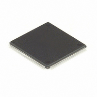
MC68HC16Z1CAG25 Freescale Semiconductor, MC68HC16Z1CAG25 Datasheet - Page 180

MC68HC16Z1CAG25
Manufacturer Part Number
MC68HC16Z1CAG25
Description
IC MCU 16BIT 25MHZ 144-LQFP
Manufacturer
Freescale Semiconductor
Series
HC16r
Datasheet
1.MC68HC16Z1VEH16.pdf
(500 pages)
Specifications of MC68HC16Z1CAG25
Core Processor
CPU16
Core Size
16-Bit
Speed
25MHz
Connectivity
EBI/EMI, SCI, SPI
Peripherals
POR, PWM, WDT
Number Of I /o
16
Program Memory Type
ROMless
Ram Size
1K x 8
Voltage - Supply (vcc/vdd)
2.7 V ~ 5.5 V
Data Converters
A/D 8x10b
Oscillator Type
Internal
Operating Temperature
-40°C ~ 85°C
Package / Case
144-LQFP
Cpu Family
HC16
Device Core Size
16b
Frequency (max)
25MHz
Interface Type
SCI/SPI/UART
Program Memory Size
Not Required
Total Internal Ram Size
1KB
# I/os (max)
16
Number Of Timers - General Purpose
11
Operating Supply Voltage (typ)
3.3/5V
Operating Supply Voltage (max)
5.5V
Operating Supply Voltage (min)
2.7V
On-chip Adc
8-chx10-bit
Instruction Set Architecture
CISC
Operating Temp Range
-40C to 85C
Operating Temperature Classification
Industrial
Mounting
Surface Mount
Pin Count
144
Package Type
LQFP
Controller Family/series
68HC16
No. Of I/o's
16
Ram Memory Size
1KB
Cpu Speed
25MHz
No. Of Timers
2
Embedded Interface Type
QSPI, SCI
Rohs Compliant
Yes
Processor Series
HC16Z
Core
CPU16
Data Bus Width
16 bit
Data Ram Size
1 KB
Maximum Clock Frequency
25 MHz
Number Of Programmable I/os
16
Number Of Timers
11
Maximum Operating Temperature
+ 85 C
Mounting Style
SMD/SMT
Minimum Operating Temperature
- 40 C
Lead Free Status / RoHS Status
Lead free / RoHS Compliant
Eeprom Size
-
Program Memory Size
-
Lead Free Status / Rohs Status
Compliant
Available stocks
Company
Part Number
Manufacturer
Quantity
Price
Company:
Part Number:
MC68HC16Z1CAG25
Manufacturer:
FREESCAL
Quantity:
455
Company:
Part Number:
MC68HC16Z1CAG25
Manufacturer:
Freescale Semiconductor
Quantity:
10 000
- Current page: 180 of 500
- Download datasheet (6Mb)
6.2 SRAM Array Address Mapping
6.3 SRAM Array Address Space Type
6.4 Normal Access
6.5 Standby and Low-Power Stop Operation
6-2
Base address registers RAMBAH and RAMBAL are used to specify the SRAM array
base address in the memory map. RAMBAH and RAMBAL can only be written while
the SRAM is in low-power stop mode (RAMMCR STOP = 1) and the base address lock
(RAMMCR RLCK = 0) is disabled. RLCK can be written once only to a value of one;
subsequent writes are ignored. This prevents accidental remapping of the array.
The RASP[1:0] in RAMMCR determine the SRAM array address space type. The
SRAM module can respond to both program and data space accesses or to program
space accesses only. Because the CPU16 operates in supervisor mode only, RASP1
has no effect.
Refer to
types and program/data space access. Refer to
formation on addressing modes.
The array can be accessed by byte, word, or long word. A byte or aligned word access
takes one bus cycle or two system clocks. A long word or misaligned word access re-
quires two bus cycles. Refer to
access times.
Standby and low-power modes should not be confused. Standby mode maintains the
RAM array when the main MCU power supply is turned off. Low-power stop mode al-
lows the CPU16 to control MCU power consumption by disabling unused modules.
Relative voltage levels of the MCU V
is in standby mode. SRAM circuitry switches to the standby power source when V
drops below specified limits. If specified standby supply voltage levels are maintained
during the transition, there is no loss of memory when switching occurs. The RAM ar-
ray cannot be accessed while the SRAM module is powered from V
operation is not desired, connect the V
5.5.1.7 Function Codes
In the CPU16, ADDR[23:20] follow the logic state of ADDR19. The
SRAM array must not be mapped to addresses $080000–$7FFFFF,
which are inaccessible to the CPU16. If mapped to these addresses,
the array remains inaccessible until a reset occurs, or it is remapped
outside of this range.
Table 6-2
Table 6-2 SRAM Array Address Space Type
Freescale Semiconductor, Inc.
RASP[1:0]
For More Information On This Product,
shows RASP[1:0] encodings.
X0
X1
STANDBY RAM MODULE
Go to: www.freescale.com
5.6 Bus Operation
for more information concerning address space
DD
Program and data accesses
STBY
and V
Program access only
NOTE
pin to V
STBY
Space
4.6 Addressing Modes
pins determine whether the SRAM
SS
for more information concerning
.
M68HC16 Z SERIES
STBY
USER’S MANUAL
for more in-
. If standby
DD
Related parts for MC68HC16Z1CAG25
Image
Part Number
Description
Manufacturer
Datasheet
Request
R
Part Number:
Description:
Manufacturer:
Freescale Semiconductor, Inc
Datasheet:
Part Number:
Description:
Manufacturer:
Freescale Semiconductor, Inc
Datasheet:
Part Number:
Description:
Manufacturer:
Freescale Semiconductor, Inc
Datasheet:
Part Number:
Description:
Manufacturer:
Freescale Semiconductor, Inc
Datasheet:
Part Number:
Description:
Manufacturer:
Freescale Semiconductor, Inc
Datasheet:
Part Number:
Description:
Manufacturer:
Freescale Semiconductor, Inc
Datasheet:
Part Number:
Description:
Manufacturer:
Freescale Semiconductor, Inc
Datasheet:
Part Number:
Description:
Manufacturer:
Freescale Semiconductor, Inc
Datasheet:
Part Number:
Description:
Manufacturer:
Freescale Semiconductor, Inc
Datasheet:
Part Number:
Description:
Manufacturer:
Freescale Semiconductor, Inc
Datasheet:
Part Number:
Description:
Manufacturer:
Freescale Semiconductor, Inc
Datasheet:
Part Number:
Description:
Manufacturer:
Freescale Semiconductor, Inc
Datasheet:
Part Number:
Description:
Manufacturer:
Freescale Semiconductor, Inc
Datasheet:
Part Number:
Description:
Manufacturer:
Freescale Semiconductor, Inc
Datasheet:
Part Number:
Description:
Manufacturer:
Freescale Semiconductor, Inc
Datasheet:


