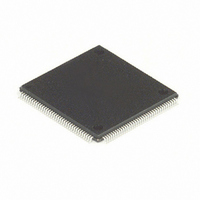
MC68HC16Z1CAG25 Freescale Semiconductor, MC68HC16Z1CAG25 Datasheet - Page 199

MC68HC16Z1CAG25
Manufacturer Part Number
MC68HC16Z1CAG25
Description
IC MCU 16BIT 25MHZ 144-LQFP
Manufacturer
Freescale Semiconductor
Series
HC16r
Datasheet
1.MC68HC16Z1VEH16.pdf
(500 pages)
Specifications of MC68HC16Z1CAG25
Core Processor
CPU16
Core Size
16-Bit
Speed
25MHz
Connectivity
EBI/EMI, SCI, SPI
Peripherals
POR, PWM, WDT
Number Of I /o
16
Program Memory Type
ROMless
Ram Size
1K x 8
Voltage - Supply (vcc/vdd)
2.7 V ~ 5.5 V
Data Converters
A/D 8x10b
Oscillator Type
Internal
Operating Temperature
-40°C ~ 85°C
Package / Case
144-LQFP
Cpu Family
HC16
Device Core Size
16b
Frequency (max)
25MHz
Interface Type
SCI/SPI/UART
Program Memory Size
Not Required
Total Internal Ram Size
1KB
# I/os (max)
16
Number Of Timers - General Purpose
11
Operating Supply Voltage (typ)
3.3/5V
Operating Supply Voltage (max)
5.5V
Operating Supply Voltage (min)
2.7V
On-chip Adc
8-chx10-bit
Instruction Set Architecture
CISC
Operating Temp Range
-40C to 85C
Operating Temperature Classification
Industrial
Mounting
Surface Mount
Pin Count
144
Package Type
LQFP
Controller Family/series
68HC16
No. Of I/o's
16
Ram Memory Size
1KB
Cpu Speed
25MHz
No. Of Timers
2
Embedded Interface Type
QSPI, SCI
Rohs Compliant
Yes
Processor Series
HC16Z
Core
CPU16
Data Bus Width
16 bit
Data Ram Size
1 KB
Maximum Clock Frequency
25 MHz
Number Of Programmable I/os
16
Number Of Timers
11
Maximum Operating Temperature
+ 85 C
Mounting Style
SMD/SMT
Minimum Operating Temperature
- 40 C
Lead Free Status / RoHS Status
Lead free / RoHS Compliant
Eeprom Size
-
Program Memory Size
-
Lead Free Status / Rohs Status
Compliant
Available stocks
Company
Part Number
Manufacturer
Quantity
Price
Company:
Part Number:
MC68HC16Z1CAG25
Manufacturer:
FREESCAL
Quantity:
455
Company:
Part Number:
MC68HC16Z1CAG25
Manufacturer:
Freescale Semiconductor
Quantity:
10 000
- Current page: 199 of 500
- Download datasheet (6Mb)
8.7.7 Successive Approximation Register
8.7.8 Result Registers
M68HC16 Z SERIES
USER’S MANUAL
The successive approximation register (SAR) accumulates the result of each conver-
sion one bit at a time, starting with the most significant bit.
At the start of the resolution period, the MSB of the SAR is set, and all less significant
bits are cleared. Depending on the result of the first comparison, the MSB is either left
set or cleared. Each successive bit is set or left cleared in descending order until all
eight or ten bits have been resolved.
When conversion is complete, the content of the SAR is transferred to the appropriate
result register. Refer to
and configuration.
Result registers are used to store data after conversion is complete. The registers can
be accessed from the IMB under ABIU control. Each register can be read from three
different addresses in the ADC memory map. The format of the result data depends
on the address from which it is read.
SAMPLE
INITIAL
TIME
CH 1
1
SAMPLE AND TRANSFER
SCF FLAG SET HERE AND SEQUENCE
TRANSFER
PERIOD
6 CYCLES
ENDS IF IN THE 4-CHANNEL MODE
TIME
CH 2
(2 ADC CLOCKS)
SAMPLE
FINAL
TIME
Freescale Semiconductor, Inc.
CH 3
Figure 8-3 10-Bit Conversion Timing
For More Information On This Product,
APPENDIX D REGISTER SUMMARY
ANALOG-TO-DIGITAL CONVERTER
CYCLES
SAR9
2
Go to: www.freescale.com
CH 4
CYCLE
SAR8
1
SUCCESSIVE APPROXIMATION
CYCLE
Table 8-9
SAR7
1
CH 5
CYCLE
SAR6
1
RESOLUTION TIME
SEQUENCE
SCF FLAG SET HERE AND SEQUENCE
CYCLE
SAR5
1
ENDS IF IN THE 8-CHANNEL MODE
shows the three types of formats.
CH 6
CYCLE
SAR4
1
CYCLE
SAR3
1
CYCLE
SAR2
CH 7
1
CYCLE
SAR1
TRANSFER CONVERSION TO
RESULT REGISTER AND SET
1
for register mapping
CYCLE
SAR0
1
CH 8
CYCLE
END
CCF
EOC
1
16
16 ADC 10-BIT TIM
8-13
Related parts for MC68HC16Z1CAG25
Image
Part Number
Description
Manufacturer
Datasheet
Request
R
Part Number:
Description:
Manufacturer:
Freescale Semiconductor, Inc
Datasheet:
Part Number:
Description:
Manufacturer:
Freescale Semiconductor, Inc
Datasheet:
Part Number:
Description:
Manufacturer:
Freescale Semiconductor, Inc
Datasheet:
Part Number:
Description:
Manufacturer:
Freescale Semiconductor, Inc
Datasheet:
Part Number:
Description:
Manufacturer:
Freescale Semiconductor, Inc
Datasheet:
Part Number:
Description:
Manufacturer:
Freescale Semiconductor, Inc
Datasheet:
Part Number:
Description:
Manufacturer:
Freescale Semiconductor, Inc
Datasheet:
Part Number:
Description:
Manufacturer:
Freescale Semiconductor, Inc
Datasheet:
Part Number:
Description:
Manufacturer:
Freescale Semiconductor, Inc
Datasheet:
Part Number:
Description:
Manufacturer:
Freescale Semiconductor, Inc
Datasheet:
Part Number:
Description:
Manufacturer:
Freescale Semiconductor, Inc
Datasheet:
Part Number:
Description:
Manufacturer:
Freescale Semiconductor, Inc
Datasheet:
Part Number:
Description:
Manufacturer:
Freescale Semiconductor, Inc
Datasheet:
Part Number:
Description:
Manufacturer:
Freescale Semiconductor, Inc
Datasheet:
Part Number:
Description:
Manufacturer:
Freescale Semiconductor, Inc
Datasheet:


