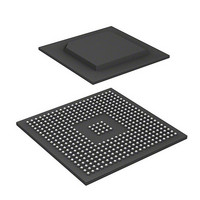
R8A77850ADBGV#RD0Z Renesas Electronics America, R8A77850ADBGV#RD0Z Datasheet - Page 547

R8A77850ADBGV#RD0Z
Manufacturer Part Number
R8A77850ADBGV#RD0Z
Description
IC SUPERH MPU ROMLESS 436-BGA
Manufacturer
Renesas Electronics America
Series
SuperH® SH7780r
Datasheet
1.R8A77850AADBGV.pdf
(1694 pages)
Specifications of R8A77850ADBGV#RD0Z
Core Processor
SH-4A
Core Size
32-Bit
Speed
600MHz
Connectivity
Audio Codec, MMC, Serial Sound, SCI, SIO, SPI, SSI
Peripherals
DMA, POR, WDT
Number Of I /o
108
Program Memory Type
ROMless
Ram Size
8K x 8
Voltage - Supply (vcc/vdd)
1 V ~ 1.2 V
Oscillator Type
External
Operating Temperature
-40°C ~ 85°C
Package / Case
436-BGA
Lead Free Status / RoHS Status
Lead free / RoHS Compliant
Eeprom Size
-
Program Memory Size
-
Data Converters
-
Available stocks
Company
Part Number
Manufacturer
Quantity
Price
Part Number:
R8A77850ADBGV#RD0ZR8A77850ADBGV
Manufacturer:
Renesas Electronics America
Quantity:
10 000
- Current page: 547 of 1694
- Download datasheet (9Mb)
command to be issued at time 2 from the following request queue. From the search results it is
seen that advance precharge processing can be executed for the third read (8-byte) request and the
fourth read (16-byte) request. Because the DBSC2 gives priority to preceding requests, it decides
to perform advance precharge processing for the third read (8-byte) request, and issues a PRE
command to the SDRAM.
When the time advances to time 3, the ACT command cannot be issued for the first read (16-byte)
request at time 3 either, and so a search of the following queue is performed for a command which
can be issued. Due to timing constraints, the ACT command cannot be issued for the third read (8-
byte) request, and as a result, issuance of the PRE command corresponding to the fourth read (16-
byte) request is selected.
At time 4, it is possible to execute request processing for the first read (16-byte) request, and an
ACT command is issued to the DDR2-SDRAM.
Thereafter, the processing described above is repeated.
Request
No.
1
2
3
4
SDRAM command
Read (16 bytes)
Read (32 bytes)
Read (8 bytes)
Read (16 bytes)
Request
Figure 12.6 Example of Preceding Precharge/Activate Processing
Bank to be
accessed
Bank 0
Bank 1
Bank 2
Bank 3
Page state
during request
Miss
Hit
Miss
Miss
As the burst length is 4 in the DDR2-SDRAM, the interval between READ commands is always two cycles.
PRE
PRE PRE
Time Time Time Time Time Time Time Time Time Time Time Time Time Time Time
1
PRE
2
PRE ACT
PRE
3
ACT
4
5
ACT READ ACT READ
ACT
6
READ
Rev.1.00 Jan. 10, 2008 Page 515 of 1658
7
ACT
12. DDR2-SDRAM Interface (DBSC2)
8
READ
9
10
READ
READ
11
12
REJ09B0261-0100
READ
READ
13
14
READ
READ
15
Related parts for R8A77850ADBGV#RD0Z
Image
Part Number
Description
Manufacturer
Datasheet
Request
R

Part Number:
Description:
KIT STARTER FOR M16C/29
Manufacturer:
Renesas Electronics America
Datasheet:

Part Number:
Description:
KIT STARTER FOR R8C/2D
Manufacturer:
Renesas Electronics America
Datasheet:

Part Number:
Description:
R0K33062P STARTER KIT
Manufacturer:
Renesas Electronics America
Datasheet:

Part Number:
Description:
KIT STARTER FOR R8C/23 E8A
Manufacturer:
Renesas Electronics America
Datasheet:

Part Number:
Description:
KIT STARTER FOR R8C/25
Manufacturer:
Renesas Electronics America
Datasheet:

Part Number:
Description:
KIT STARTER H8S2456 SHARPE DSPLY
Manufacturer:
Renesas Electronics America
Datasheet:

Part Number:
Description:
KIT STARTER FOR R8C38C
Manufacturer:
Renesas Electronics America
Datasheet:

Part Number:
Description:
KIT STARTER FOR R8C35C
Manufacturer:
Renesas Electronics America
Datasheet:

Part Number:
Description:
KIT STARTER FOR R8CL3AC+LCD APPS
Manufacturer:
Renesas Electronics America
Datasheet:

Part Number:
Description:
KIT STARTER FOR RX610
Manufacturer:
Renesas Electronics America
Datasheet:

Part Number:
Description:
KIT STARTER FOR R32C/118
Manufacturer:
Renesas Electronics America
Datasheet:

Part Number:
Description:
KIT DEV RSK-R8C/26-29
Manufacturer:
Renesas Electronics America
Datasheet:

Part Number:
Description:
KIT STARTER FOR SH7124
Manufacturer:
Renesas Electronics America
Datasheet:

Part Number:
Description:
KIT STARTER FOR H8SX/1622
Manufacturer:
Renesas Electronics America
Datasheet:

Part Number:
Description:
KIT DEV FOR SH7203
Manufacturer:
Renesas Electronics America
Datasheet:


