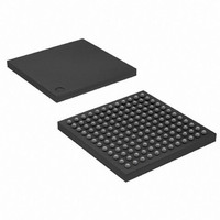
AT91SAM7SE256-CU Atmel, AT91SAM7SE256-CU Datasheet - Page 280

AT91SAM7SE256-CU
Manufacturer Part Number
AT91SAM7SE256-CU
Description
IC ARM7 MCU FLASH 256K 144-LFBGA
Manufacturer
Atmel
Series
AT91SAMr
Datasheet
1.AT91SAM7SE256-AU.pdf
(673 pages)
Specifications of AT91SAM7SE256-CU
Core Processor
ARM7
Core Size
16/32-Bit
Speed
55MHz
Connectivity
EBI/EMI, I²C, SPI, SSC, UART/USART, USB
Peripherals
Brown-out Detect/Reset, POR, PWM, WDT
Number Of I /o
88
Program Memory Size
256KB (256K x 8)
Program Memory Type
FLASH
Ram Size
32K x 8
Voltage - Supply (vcc/vdd)
1.65 V ~ 1.95 V
Data Converters
A/D 8x10b
Oscillator Type
Internal
Operating Temperature
-40°C ~ 85°C
Package / Case
144-LFBGA
Processor Series
AT91SAMx
Core
ARM7TDMI
Data Bus Width
32 bit
Data Ram Size
32 KB
Interface Type
EBI, SPI, TWI, USART
Maximum Clock Frequency
48 MHz
Number Of Programmable I/os
32
Number Of Timers
3
Operating Supply Voltage
1.8 V to 3.3 V
Maximum Operating Temperature
+ 85 C
Mounting Style
SMD/SMT
3rd Party Development Tools
JTRACE-ARM-2M, KSK-AT91SAM7S-PL, MDK-ARM, RL-ARM, ULINK2
Development Tools By Supplier
AT91SAM-ICE, AT91-ISP, AT91SAM7SE-EK
Minimum Operating Temperature
- 40 C
On-chip Adc
10 bit
For Use With
AT91SAM7SE-EK - EVAL BOARD FOR AT91SAM7SEAT91SAM-ICE - EMULATOR FOR AT91 ARM7/ARM9
Lead Free Status / RoHS Status
Lead free / RoHS Compliant
Eeprom Size
-
Lead Free Status / Rohs Status
Details
Other names
AT91SAM7SE256-CJ
AT91SAM7SE256-CJ
AT91SAM7SE256-CJ
Available stocks
Company
Part Number
Manufacturer
Quantity
Price
- Current page: 280 of 673
- Download datasheet (11Mb)
input divided by PRES parameter. By default, the PRES parameter is set to 1 which means
that master clock is equal to slow clock.
Once the PMC_PCKx register has been programmed, The corresponding Programmable
clock must be enabled and the user is constrained to wait for the PCKRDYx bit to be set in
the PMC_SR register. This can be done either by polling the status register or by waiting the
interrupt line to be raised if the associated interrupt to PCKRDYx has been enabled in the
PMC_IER register. All parameters in PMC_PCKx can be programmed in a single write
operation.
If the CSS and PRES parameters are to be modified, the corresponding Programmable
clock must be disabled first. The parameters can then be modified. Once this has been
done, the user must re-enable the Programmable clock and wait for the PCKRDYx bit to be
set.
Code Example:
write_register(PMC_PCK0,0x00000015)
Programmable clock 0 is main clock divided by 32.
6. Enabling Peripheral Clocks
Once all of the previous steps have been completed, the peripheral clocks can be enabled
and/or disabled via registers PMC_PCER and PMC_PCDR.
Depending on the system used, AT91SAM7SE512,14 peripheral clocks and for
AT91SAM7SE256/32,12 peripheral clocks can be enabled or disabled. The PMC_PCSR
provides a clear view as to which peripheral clock is enabled.
Note:
Each enabled peripheral clock corresponds to Master Clock.
Code Examples:
write_register(PMC_PCER,0x00000110)
Peripheral clocks 4 and 8 are enabled.
write_register(PMC_PCDR,0x00000010)
Peripheral clock 4 is disabled.
SAM7SE512/256/32 Preliminary
280
6222F–ATARM–14-Jan-11
Related parts for AT91SAM7SE256-CU
Image
Part Number
Description
Manufacturer
Datasheet
Request
R

Part Number:
Description:
EVAL BOARD FOR AT91SAM7SE
Manufacturer:
Atmel
Datasheet:

Part Number:
Description:
KIT EVAL FOR ARM AT91SAM7S
Manufacturer:
Atmel
Datasheet:

Part Number:
Description:
MCU, MPU & DSP Development Tools KICKSTART KIT ATMEL AT91SAM7S
Manufacturer:
IAR Systems

Part Number:
Description:
MCU ARM9 64K SRAM 144-LFBGA
Manufacturer:
Atmel
Datasheet:

Part Number:
Description:
IC ARM7 MCU FLASH 256K 100LQFP
Manufacturer:
Atmel
Datasheet:

Part Number:
Description:
IC ARM9 MPU 217-LFBGA
Manufacturer:
Atmel
Datasheet:

Part Number:
Description:
MCU ARM9 ULTRA LOW PWR 217-LFBGA
Manufacturer:
Atmel
Datasheet:

Part Number:
Description:
MCU ARM9 324-TFBGA
Manufacturer:
Atmel
Datasheet:

Part Number:
Description:
IC MCU ARM9 SAMPLING 217CBGA
Manufacturer:
Atmel
Datasheet:

Part Number:
Description:
IC ARM9 MCU 217-LFBGA
Manufacturer:
Atmel
Datasheet:

Part Number:
Description:
IC ARM9 MCU 208-PQFP
Manufacturer:
Atmel
Datasheet:

Part Number:
Description:
MCU ARM 512K HS FLASH 100-LQFP
Manufacturer:
Atmel
Datasheet:

Part Number:
Description:
MCU ARM 512K HS FLASH 100-TFBGA
Manufacturer:
Atmel
Datasheet:

Part Number:
Description:
IC ARM9 MCU 200 MHZ 324-TFBGA
Manufacturer:
Atmel
Datasheet:

Part Number:
Description:
IC ARM MCU 16BIT 128K 256BGA
Manufacturer:
Atmel
Datasheet:


