AT91SAM7SE256-CU Atmel, AT91SAM7SE256-CU Datasheet - Page 654
AT91SAM7SE256-CU
Manufacturer Part Number
AT91SAM7SE256-CU
Description
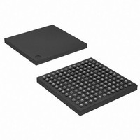
IC ARM7 MCU FLASH 256K 144-LFBGA
Manufacturer
Atmel
Series
AT91SAMr
Datasheet
1.AT91SAM7SE256-AU.pdf
(673 pages)
Specifications of AT91SAM7SE256-CU
Core Processor
ARM7
Core Size
16/32-Bit
Speed
55MHz
Connectivity
EBI/EMI, I²C, SPI, SSC, UART/USART, USB
Peripherals
Brown-out Detect/Reset, POR, PWM, WDT
Number Of I /o
88
Program Memory Size
256KB (256K x 8)
Program Memory Type
FLASH
Ram Size
32K x 8
Voltage - Supply (vcc/vdd)
1.65 V ~ 1.95 V
Data Converters
A/D 8x10b
Oscillator Type
Internal
Operating Temperature
-40°C ~ 85°C
Package / Case
144-LFBGA
Processor Series
AT91SAMx
Core
ARM7TDMI
Data Bus Width
32 bit
Data Ram Size
32 KB
Interface Type
EBI, SPI, TWI, USART
Maximum Clock Frequency
48 MHz
Number Of Programmable I/os
32
Number Of Timers
3
Operating Supply Voltage
1.8 V to 3.3 V
Maximum Operating Temperature
+ 85 C
Mounting Style
SMD/SMT
3rd Party Development Tools
JTRACE-ARM-2M, KSK-AT91SAM7S-PL, MDK-ARM, RL-ARM, ULINK2
Development Tools By Supplier
AT91SAM-ICE, AT91-ISP, AT91SAM7SE-EK
Minimum Operating Temperature
- 40 C
On-chip Adc
10 bit
For Use With
AT91SAM7SE-EK - EVAL BOARD FOR AT91SAM7SEAT91SAM-ICE - EMULATOR FOR AT91 ARM7/ARM9
Lead Free Status / RoHS Status
Lead free / RoHS Compliant
Eeprom Size
-
Lead Free Status / Rohs Status
Details
Other names
AT91SAM7SE256-CJ
AT91SAM7SE256-CJ
AT91SAM7SE256-CJ
Available stocks
Company
Part Number
Manufacturer
Quantity
Price


43.2.2
43.2.2.1
43.2.3
43.2.3.1
43.2.3.2
43.2.3.3
43.2.3.4
43.2.4
43.2.4.1
654
SAM7SE512/256/32 Preliminary
Flash Memory
Pulse Width Modulation Controller (PWM)
Real-Time Timer (RTT)
Flash: Power Consumption with data read access with multiple load of two words
PWM: Update when PWM_CCNTx = 0 or 1
PWM: Update when PWM_CPRDx = 0
PWM: Counter Start Value
PWM: Behavior of CHIDx Status Bits in the PWM_SR Register
RTT: Possible Event Loss when Reading RTT_SR
When no Wait State (FWS = 0) is programmed and when data read access is performed with a
multiple load of two words, the internal Flash may stay in read mode.
It implies a potential increase of power consumption on VDDCORE (around 2 mA). Note that it
does not concern the program execution; thus, no issue is present when the program is fetching
out of Flash.
2 workarounds are possible:
If the Channel Counter Register value is 0 or 1, the Channel Period Register or Channel Duty
Cycle Register is directly modified when writing the Channel Update Register.
Check the Channel Counter Register before writing the Channel Update Register.
When the Channel Period Register equals 0, the period update is not operational.
Do not write 0 in the Channel Period Register.
In left aligned mode, the first start value of the counter is 0. For the other periods, the counter
starts at 1.
None.
Erratic behavior of the CHIDx status bit in the PWM_SR Register. When a channel is disabled
by writing in the PWM_DIS Register just after enabling it (before completion of a Clock Period of
the clock selected for the channel), the PWM line is internally disabled but the CHIDx status bit
in the PWM_SR stays at 1.
Do not disable a channel before completion of one period of the selected clock.
If an event (RTTINC or ALMS) occurs within the same slow clock cycle that RTT_SR is read, the
corresponding bit might be cleared. This might lead to the loss of this event.
• Add one Wait State when performing these data read accesses (FWS =1)
• After the multiple load, perform a single read data access to an address different from the
previous address accesses.
Problem Fix/Workaround
Problem Fix/Workaround
Problem Fix/Workaround
Problem Fix/Workaround
Problem Fix/Workaround
6222F–ATARM–14-Jan-11
Related parts for AT91SAM7SE256-CU
Image
Part Number
Description
Manufacturer
Datasheet
Request
R

Part Number:
Description:
EVAL BOARD FOR AT91SAM7SE
Manufacturer:
Atmel
Datasheet:

Part Number:
Description:
KIT EVAL FOR ARM AT91SAM7S
Manufacturer:
Atmel
Datasheet:

Part Number:
Description:
MCU, MPU & DSP Development Tools KICKSTART KIT ATMEL AT91SAM7S
Manufacturer:
IAR Systems

Part Number:
Description:
MCU ARM9 64K SRAM 144-LFBGA
Manufacturer:
Atmel
Datasheet:

Part Number:
Description:
IC ARM7 MCU FLASH 256K 100LQFP
Manufacturer:
Atmel
Datasheet:

Part Number:
Description:
IC ARM9 MPU 217-LFBGA
Manufacturer:
Atmel
Datasheet:
Part Number:
Description:
MCU ARM9 ULTRA LOW PWR 217-LFBGA
Manufacturer:
Atmel
Datasheet:

Part Number:
Description:
MCU ARM9 324-TFBGA
Manufacturer:
Atmel
Datasheet:
Part Number:
Description:
IC MCU ARM9 SAMPLING 217CBGA
Manufacturer:
Atmel
Datasheet:
Part Number:
Description:
IC ARM9 MCU 217-LFBGA
Manufacturer:
Atmel
Datasheet:

Part Number:
Description:
IC ARM9 MCU 208-PQFP
Manufacturer:
Atmel
Datasheet:
Part Number:
Description:
MCU ARM 512K HS FLASH 100-LQFP
Manufacturer:
Atmel
Datasheet:

Part Number:
Description:
MCU ARM 512K HS FLASH 100-TFBGA
Manufacturer:
Atmel
Datasheet:
Part Number:
Description:
IC ARM9 MCU 200 MHZ 324-TFBGA
Manufacturer:
Atmel
Datasheet:

Part Number:
Description:
IC ARM MCU 16BIT 128K 256BGA
Manufacturer:
Atmel
Datasheet: