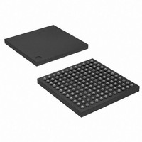
AT91SAM7SE256-CU Atmel, AT91SAM7SE256-CU Datasheet - Page 504

AT91SAM7SE256-CU
Manufacturer Part Number
AT91SAM7SE256-CU
Description
IC ARM7 MCU FLASH 256K 144-LFBGA
Manufacturer
Atmel
Series
AT91SAMr
Datasheet
1.AT91SAM7SE256-AU.pdf
(673 pages)
Specifications of AT91SAM7SE256-CU
Core Processor
ARM7
Core Size
16/32-Bit
Speed
55MHz
Connectivity
EBI/EMI, I²C, SPI, SSC, UART/USART, USB
Peripherals
Brown-out Detect/Reset, POR, PWM, WDT
Number Of I /o
88
Program Memory Size
256KB (256K x 8)
Program Memory Type
FLASH
Ram Size
32K x 8
Voltage - Supply (vcc/vdd)
1.65 V ~ 1.95 V
Data Converters
A/D 8x10b
Oscillator Type
Internal
Operating Temperature
-40°C ~ 85°C
Package / Case
144-LFBGA
Processor Series
AT91SAMx
Core
ARM7TDMI
Data Bus Width
32 bit
Data Ram Size
32 KB
Interface Type
EBI, SPI, TWI, USART
Maximum Clock Frequency
48 MHz
Number Of Programmable I/os
32
Number Of Timers
3
Operating Supply Voltage
1.8 V to 3.3 V
Maximum Operating Temperature
+ 85 C
Mounting Style
SMD/SMT
3rd Party Development Tools
JTRACE-ARM-2M, KSK-AT91SAM7S-PL, MDK-ARM, RL-ARM, ULINK2
Development Tools By Supplier
AT91SAM-ICE, AT91-ISP, AT91SAM7SE-EK
Minimum Operating Temperature
- 40 C
On-chip Adc
10 bit
For Use With
AT91SAM7SE-EK - EVAL BOARD FOR AT91SAM7SEAT91SAM-ICE - EMULATOR FOR AT91 ARM7/ARM9
Lead Free Status / RoHS Status
Lead free / RoHS Compliant
Eeprom Size
-
Lead Free Status / Rohs Status
Details
Other names
AT91SAM7SE256-CJ
AT91SAM7SE256-CJ
AT91SAM7SE256-CJ
Available stocks
Company
Part Number
Manufacturer
Quantity
Price
- Current page: 504 of 673
- Download datasheet (11Mb)
36.5
36.5.1
36.5.1.1
36.5.1.2
504
Functional Description
SAM7SE512/256/32 Preliminary
TC Description
16-bit Counter
Clock Selection
The three channels of the Timer/Counter are independent and identical in operation. The regis-
ters for channel programming are listed in
Each channel is organized around a 16-bit counter. The value of the counter is incremented at
each positive edge of the selected clock. When the counter has reached the value 0xFFFF and
passes to 0x0000, an overflow occurs and the COVFS bit in TC_SR (Status Register) is set.
The current value of the counter is accessible in real time by reading the Counter Value Regis-
ter, TC_CV. The counter can be reset by a trigger. In this case, the counter value passes to
0x0000 on the next valid edge of the selected clock.
At block level, input clock signals of each channel can either be connected to the external inputs
TCLK0, TCLK1 or TCLK2, or be connected to the configurable I/O signals TIOA0, TIOA1 or
TIOA2 for chaining by programming the TC_BMR (Block Mode). See
Each channel can independently select an internal or external clock source for its counter:
This selection is made by the TCCLKS bits in the TC Channel Mode Register.
The selected clock can be inverted with the CLKI bit in TC_CMR. This allows counting on the
opposite edges of the clock.
The burst function allows the clock to be validated when an external signal is high. The BURST
parameter in the Mode Register defines this signal (none, XC0, XC1, XC2). See
page
Note:
• Internal clock signals: TIMER_CLOCK1, TIMER_CLOCK2, TIMER_CLOCK3,
• External clock signals: XC0, XC1 or XC2
TIMER_CLOCK4, TIMER_CLOCK5
505.
In all cases, if an external clock is used, the duration of each of its levels must be longer than the
master clock period. The external clock frequency must be at least 2.5 times lower than the mas-
ter clock.
Table 36-4 on page
517.
Figure 36-2 on page
6222F–ATARM–14-Jan-11
Figure 36-3 on
505.
Related parts for AT91SAM7SE256-CU
Image
Part Number
Description
Manufacturer
Datasheet
Request
R

Part Number:
Description:
EVAL BOARD FOR AT91SAM7SE
Manufacturer:
Atmel
Datasheet:

Part Number:
Description:
KIT EVAL FOR ARM AT91SAM7S
Manufacturer:
Atmel
Datasheet:

Part Number:
Description:
MCU, MPU & DSP Development Tools KICKSTART KIT ATMEL AT91SAM7S
Manufacturer:
IAR Systems

Part Number:
Description:
MCU ARM9 64K SRAM 144-LFBGA
Manufacturer:
Atmel
Datasheet:

Part Number:
Description:
IC ARM7 MCU FLASH 256K 100LQFP
Manufacturer:
Atmel
Datasheet:

Part Number:
Description:
IC ARM9 MPU 217-LFBGA
Manufacturer:
Atmel
Datasheet:

Part Number:
Description:
MCU ARM9 ULTRA LOW PWR 217-LFBGA
Manufacturer:
Atmel
Datasheet:

Part Number:
Description:
MCU ARM9 324-TFBGA
Manufacturer:
Atmel
Datasheet:

Part Number:
Description:
IC MCU ARM9 SAMPLING 217CBGA
Manufacturer:
Atmel
Datasheet:

Part Number:
Description:
IC ARM9 MCU 217-LFBGA
Manufacturer:
Atmel
Datasheet:

Part Number:
Description:
IC ARM9 MCU 208-PQFP
Manufacturer:
Atmel
Datasheet:

Part Number:
Description:
MCU ARM 512K HS FLASH 100-LQFP
Manufacturer:
Atmel
Datasheet:

Part Number:
Description:
MCU ARM 512K HS FLASH 100-TFBGA
Manufacturer:
Atmel
Datasheet:

Part Number:
Description:
IC ARM9 MCU 200 MHZ 324-TFBGA
Manufacturer:
Atmel
Datasheet:

Part Number:
Description:
IC ARM MCU 16BIT 128K 256BGA
Manufacturer:
Atmel
Datasheet:


