AT91SAM7SE256-CU Atmel, AT91SAM7SE256-CU Datasheet - Page 351
AT91SAM7SE256-CU
Manufacturer Part Number
AT91SAM7SE256-CU
Description
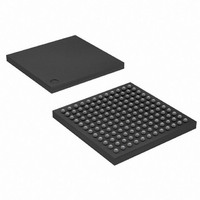
IC ARM7 MCU FLASH 256K 144-LFBGA
Manufacturer
Atmel
Series
AT91SAMr
Datasheet
1.AT91SAM7SE256-AU.pdf
(673 pages)
Specifications of AT91SAM7SE256-CU
Core Processor
ARM7
Core Size
16/32-Bit
Speed
55MHz
Connectivity
EBI/EMI, I²C, SPI, SSC, UART/USART, USB
Peripherals
Brown-out Detect/Reset, POR, PWM, WDT
Number Of I /o
88
Program Memory Size
256KB (256K x 8)
Program Memory Type
FLASH
Ram Size
32K x 8
Voltage - Supply (vcc/vdd)
1.65 V ~ 1.95 V
Data Converters
A/D 8x10b
Oscillator Type
Internal
Operating Temperature
-40°C ~ 85°C
Package / Case
144-LFBGA
Processor Series
AT91SAMx
Core
ARM7TDMI
Data Bus Width
32 bit
Data Ram Size
32 KB
Interface Type
EBI, SPI, TWI, USART
Maximum Clock Frequency
48 MHz
Number Of Programmable I/os
32
Number Of Timers
3
Operating Supply Voltage
1.8 V to 3.3 V
Maximum Operating Temperature
+ 85 C
Mounting Style
SMD/SMT
3rd Party Development Tools
JTRACE-ARM-2M, KSK-AT91SAM7S-PL, MDK-ARM, RL-ARM, ULINK2
Development Tools By Supplier
AT91SAM-ICE, AT91-ISP, AT91SAM7SE-EK
Minimum Operating Temperature
- 40 C
On-chip Adc
10 bit
For Use With
AT91SAM7SE-EK - EVAL BOARD FOR AT91SAM7SEAT91SAM-ICE - EMULATOR FOR AT91 ARM7/ARM9
Lead Free Status / RoHS Status
Lead free / RoHS Compliant
Eeprom Size
-
Lead Free Status / Rohs Status
Details
Other names
AT91SAM7SE256-CJ
AT91SAM7SE256-CJ
AT91SAM7SE256-CJ
Available stocks
Company
Part Number
Manufacturer
Quantity
Price


32.5
32.5.1
32.5.2
32.5.3
6222F–ATARM–14-Jan-11
Product Dependencies
I/O Lines
Power Management
Interrupt
Both TWD and TWCK are bidirectional lines, connected to a positive supply voltage via a current
source or pull-up resistor (see
high. The output stages of devices connected to the bus must have an open-drain or open-col-
lector to perform the wired-AND function.
TWD and TWCK pins may be multiplexed with PIO lines. To enable the TWI, the programmer
must perform the following steps:
The TWI interface may be clocked through the Power Management Controller (PMC), thus the
programmer must first configure the PMC to enable the TWI clock.
The TWI interface has an interrupt line connected to the Advanced Interrupt Controller (AIC). In
order to handle interrupts, the AIC must be programmed before configuring the TWI.
• Program the PIO controller to:
• Enable the peripheral clock.
– Dedicate TWD and TWCK as peripheral lines.
– Define TWD and TWCK as open-drain.
Figure 32-2 on page
SAM7SE512/256/32 Preliminary
350). When the bus is free, both lines are
351
Related parts for AT91SAM7SE256-CU
Image
Part Number
Description
Manufacturer
Datasheet
Request
R

Part Number:
Description:
EVAL BOARD FOR AT91SAM7SE
Manufacturer:
Atmel
Datasheet:

Part Number:
Description:
KIT EVAL FOR ARM AT91SAM7S
Manufacturer:
Atmel
Datasheet:

Part Number:
Description:
MCU, MPU & DSP Development Tools KICKSTART KIT ATMEL AT91SAM7S
Manufacturer:
IAR Systems

Part Number:
Description:
MCU ARM9 64K SRAM 144-LFBGA
Manufacturer:
Atmel
Datasheet:

Part Number:
Description:
IC ARM7 MCU FLASH 256K 100LQFP
Manufacturer:
Atmel
Datasheet:

Part Number:
Description:
IC ARM9 MPU 217-LFBGA
Manufacturer:
Atmel
Datasheet:
Part Number:
Description:
MCU ARM9 ULTRA LOW PWR 217-LFBGA
Manufacturer:
Atmel
Datasheet:

Part Number:
Description:
MCU ARM9 324-TFBGA
Manufacturer:
Atmel
Datasheet:
Part Number:
Description:
IC MCU ARM9 SAMPLING 217CBGA
Manufacturer:
Atmel
Datasheet:
Part Number:
Description:
IC ARM9 MCU 217-LFBGA
Manufacturer:
Atmel
Datasheet:

Part Number:
Description:
IC ARM9 MCU 208-PQFP
Manufacturer:
Atmel
Datasheet:
Part Number:
Description:
MCU ARM 512K HS FLASH 100-LQFP
Manufacturer:
Atmel
Datasheet:

Part Number:
Description:
MCU ARM 512K HS FLASH 100-TFBGA
Manufacturer:
Atmel
Datasheet:
Part Number:
Description:
IC ARM9 MCU 200 MHZ 324-TFBGA
Manufacturer:
Atmel
Datasheet:

Part Number:
Description:
IC ARM MCU 16BIT 128K 256BGA
Manufacturer:
Atmel
Datasheet: