AT91SAM7SE256-CU Atmel, AT91SAM7SE256-CU Datasheet - Page 657
AT91SAM7SE256-CU
Manufacturer Part Number
AT91SAM7SE256-CU
Description
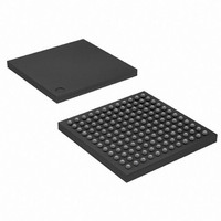
IC ARM7 MCU FLASH 256K 144-LFBGA
Manufacturer
Atmel
Series
AT91SAMr
Datasheet
1.AT91SAM7SE256-AU.pdf
(673 pages)
Specifications of AT91SAM7SE256-CU
Core Processor
ARM7
Core Size
16/32-Bit
Speed
55MHz
Connectivity
EBI/EMI, I²C, SPI, SSC, UART/USART, USB
Peripherals
Brown-out Detect/Reset, POR, PWM, WDT
Number Of I /o
88
Program Memory Size
256KB (256K x 8)
Program Memory Type
FLASH
Ram Size
32K x 8
Voltage - Supply (vcc/vdd)
1.65 V ~ 1.95 V
Data Converters
A/D 8x10b
Oscillator Type
Internal
Operating Temperature
-40°C ~ 85°C
Package / Case
144-LFBGA
Processor Series
AT91SAMx
Core
ARM7TDMI
Data Bus Width
32 bit
Data Ram Size
32 KB
Interface Type
EBI, SPI, TWI, USART
Maximum Clock Frequency
48 MHz
Number Of Programmable I/os
32
Number Of Timers
3
Operating Supply Voltage
1.8 V to 3.3 V
Maximum Operating Temperature
+ 85 C
Mounting Style
SMD/SMT
3rd Party Development Tools
JTRACE-ARM-2M, KSK-AT91SAM7S-PL, MDK-ARM, RL-ARM, ULINK2
Development Tools By Supplier
AT91SAM-ICE, AT91-ISP, AT91SAM7SE-EK
Minimum Operating Temperature
- 40 C
On-chip Adc
10 bit
For Use With
AT91SAM7SE-EK - EVAL BOARD FOR AT91SAM7SEAT91SAM-ICE - EMULATOR FOR AT91 ARM7/ARM9
Lead Free Status / RoHS Status
Lead free / RoHS Compliant
Eeprom Size
-
Lead Free Status / Rohs Status
Details
Other names
AT91SAM7SE256-CJ
AT91SAM7SE256-CJ
AT91SAM7SE256-CJ
Available stocks
Company
Part Number
Manufacturer
Quantity
Price


43.2.7.5
43.2.8
43.2.8.1
43.2.9
43.2.9.1
43.2.9.2
43.2.9.3
6222F–ATARM–14-Jan-11
Two Wire Interface (TWI)
Universal Synchronous Asynchronous Receiver Transmitter (USART)
TWI: Switching from Slave to Master Mode
USART: Two Characters Sent with Hardware Handshaking
USART: DCD is Active High Instead of Low
SSC: First RK Clock Cycle when Rk Outputs a Clock During Data Transfer
USART: CTS in Hardware Handshaking
At the end of the data, the RK pin is set in high impedance which might be seen as an unex-
pected clock cycle.
Enable the pull-up on RK pin.
When the SSC receiver is used with the following conditions:
The first clock cycle time generated by the RK pin is equal to MCK/(2 x (value +1)).
None.
When the TWI is set in slave mode and if a master write access is performed, the start event is
correctly generated but the SCL line is stuck at 1, so no transfer is possible.
Two software workarounds are possible:
When Hardware Handshaking is used and if CTS goes high near the end of the starting bit, a
character can be lost.
CTS must not go high during a time slot occurring between 2 Master Clock periods before the
starting bit and 16 Master Clock periods after the rising edge of the starting bit.
None.
When Hardware Handshaking is used and if CTS goes high during the TX of a character and if
the holding register (US_THR) is not empty, the content of the US_THR will also be transmitted.
Don’t use the PDC in transmit mode and do not fill US_THR before TXRDY is set at 1.
DCD signal is active at “High” level in USART block (Modem Mode).
DCD should be active at “Low” level.
• RX clock is divided clock (CKS = 0 and DIV different from 0)
• RK pin set as output and provides the clock during data transfer (CKO = 2)
• data sampled on RK falling edge (CKI = 0),
1. Perform a software reset before going to master mode (TWI must be reconfigured).
2. Perform a slave read access before switching to master mode.
Problem Fix/Workaround
Problem Fix/Workaround
Problem Fix/Workaround
Problem Fix/Workaround
Problem Fix/Workaround
Problem Fix/Workaround
SAM7SE512/256/32 Preliminary
657
Related parts for AT91SAM7SE256-CU
Image
Part Number
Description
Manufacturer
Datasheet
Request
R

Part Number:
Description:
EVAL BOARD FOR AT91SAM7SE
Manufacturer:
Atmel
Datasheet:

Part Number:
Description:
KIT EVAL FOR ARM AT91SAM7S
Manufacturer:
Atmel
Datasheet:

Part Number:
Description:
MCU, MPU & DSP Development Tools KICKSTART KIT ATMEL AT91SAM7S
Manufacturer:
IAR Systems

Part Number:
Description:
MCU ARM9 64K SRAM 144-LFBGA
Manufacturer:
Atmel
Datasheet:

Part Number:
Description:
IC ARM7 MCU FLASH 256K 100LQFP
Manufacturer:
Atmel
Datasheet:

Part Number:
Description:
IC ARM9 MPU 217-LFBGA
Manufacturer:
Atmel
Datasheet:
Part Number:
Description:
MCU ARM9 ULTRA LOW PWR 217-LFBGA
Manufacturer:
Atmel
Datasheet:

Part Number:
Description:
MCU ARM9 324-TFBGA
Manufacturer:
Atmel
Datasheet:
Part Number:
Description:
IC MCU ARM9 SAMPLING 217CBGA
Manufacturer:
Atmel
Datasheet:
Part Number:
Description:
IC ARM9 MCU 217-LFBGA
Manufacturer:
Atmel
Datasheet:

Part Number:
Description:
IC ARM9 MCU 208-PQFP
Manufacturer:
Atmel
Datasheet:
Part Number:
Description:
MCU ARM 512K HS FLASH 100-LQFP
Manufacturer:
Atmel
Datasheet:

Part Number:
Description:
MCU ARM 512K HS FLASH 100-TFBGA
Manufacturer:
Atmel
Datasheet:
Part Number:
Description:
IC ARM9 MCU 200 MHZ 324-TFBGA
Manufacturer:
Atmel
Datasheet:

Part Number:
Description:
IC ARM MCU 16BIT 128K 256BGA
Manufacturer:
Atmel
Datasheet: