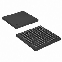
AT91SAM7SE256-CU Atmel, AT91SAM7SE256-CU Datasheet - Page 589

AT91SAM7SE256-CU
Manufacturer Part Number
AT91SAM7SE256-CU
Description
IC ARM7 MCU FLASH 256K 144-LFBGA
Manufacturer
Atmel
Series
AT91SAMr
Datasheet
1.AT91SAM7SE256-AU.pdf
(673 pages)
Specifications of AT91SAM7SE256-CU
Core Processor
ARM7
Core Size
16/32-Bit
Speed
55MHz
Connectivity
EBI/EMI, I²C, SPI, SSC, UART/USART, USB
Peripherals
Brown-out Detect/Reset, POR, PWM, WDT
Number Of I /o
88
Program Memory Size
256KB (256K x 8)
Program Memory Type
FLASH
Ram Size
32K x 8
Voltage - Supply (vcc/vdd)
1.65 V ~ 1.95 V
Data Converters
A/D 8x10b
Oscillator Type
Internal
Operating Temperature
-40°C ~ 85°C
Package / Case
144-LFBGA
Processor Series
AT91SAMx
Core
ARM7TDMI
Data Bus Width
32 bit
Data Ram Size
32 KB
Interface Type
EBI, SPI, TWI, USART
Maximum Clock Frequency
48 MHz
Number Of Programmable I/os
32
Number Of Timers
3
Operating Supply Voltage
1.8 V to 3.3 V
Maximum Operating Temperature
+ 85 C
Mounting Style
SMD/SMT
3rd Party Development Tools
JTRACE-ARM-2M, KSK-AT91SAM7S-PL, MDK-ARM, RL-ARM, ULINK2
Development Tools By Supplier
AT91SAM-ICE, AT91-ISP, AT91SAM7SE-EK
Minimum Operating Temperature
- 40 C
On-chip Adc
10 bit
For Use With
AT91SAM7SE-EK - EVAL BOARD FOR AT91SAM7SEAT91SAM-ICE - EMULATOR FOR AT91 ARM7/ARM9
Lead Free Status / RoHS Status
Lead free / RoHS Compliant
Eeprom Size
-
Lead Free Status / Rohs Status
Details
Other names
AT91SAM7SE256-CJ
AT91SAM7SE256-CJ
AT91SAM7SE256-CJ
Available stocks
Company
Part Number
Manufacturer
Quantity
Price
- Current page: 589 of 673
- Download datasheet (11Mb)
Note:
• TXCOMP: Generates an IN Packet with Data Previously Written in the DPR
This flag generates an interrupt while it is set to one.
Write (Cleared by the firmware):
0 = Clear the flag, clear the interrupt.
1 = No effect.
Read (Set by the USB peripheral):
0 = Data IN transaction has not been acknowledged by the Host.
1 = Data IN transaction is achieved, acknowledged by the Host.
After having issued a Data IN transaction setting TXPKTRDY, the device firmware waits for TXCOMP to be sure that the
host has acknowledged the transaction.
• RX_DATA_BK0: Receive Data Bank 0
This flag generates an interrupt while it is set to one.
Write (Cleared by the firmware):
0 = Notify USB peripheral device that data have been read in the FIFO's Bank 0.
1 = To leave the read value unchanged.
Read (Set by the USB peripheral):
0 = No data packet has been received in the FIFO's Bank 0.
1 = A data packet has been received, it has been stored in the FIFO's Bank 0.
When the device firmware has polled this bit or has been interrupted by this signal, it must transfer data from the FIFO to
the microcontroller memory. The number of bytes received is available in RXBYTCENT field. Bank 0 FIFO values are read
through the UDP_FDRx register. Once a transfer is done, the device firmware must release Bank 0 to the USB peripheral
device by clearing RX_DATA_BK0.
After setting or clearing this bit, a wait time of 3 UDPCK clock cycles and 3 peripheral clock cycles is required before
accessing DPR.
• RXSETUP: Received Setup
This flag generates an interrupt while it is set to one.
Read:
0 = No setup packet available.
1 = A setup data packet has been sent by the host and is available in the FIFO.
6222F–ATARM–14-Jan-11
}
In a preemptive environment, set or clear the flag and wait for a time of 1 UDPCK clock cycle and 1peripheral clock cycle. How-
ever, RX_DATA_BK0, TXPKTRDY, RX_DATA_BK1 require wait times of 3 UDPCK clock cycles and 5 peripheral clock cycles
before accessing DPR.
reg &= ~(flags); \
AT91C_BASE_UDP->UDP_CSR[endpoint] = reg; \
while ( (AT91C_BASE_UDP->UDP_CSR[endpoint] & (flags)) == (flags)); \
SAM7SE512/256/32 Preliminary
589
Related parts for AT91SAM7SE256-CU
Image
Part Number
Description
Manufacturer
Datasheet
Request
R

Part Number:
Description:
EVAL BOARD FOR AT91SAM7SE
Manufacturer:
Atmel
Datasheet:

Part Number:
Description:
KIT EVAL FOR ARM AT91SAM7S
Manufacturer:
Atmel
Datasheet:

Part Number:
Description:
MCU, MPU & DSP Development Tools KICKSTART KIT ATMEL AT91SAM7S
Manufacturer:
IAR Systems

Part Number:
Description:
MCU ARM9 64K SRAM 144-LFBGA
Manufacturer:
Atmel
Datasheet:

Part Number:
Description:
IC ARM7 MCU FLASH 256K 100LQFP
Manufacturer:
Atmel
Datasheet:

Part Number:
Description:
IC ARM9 MPU 217-LFBGA
Manufacturer:
Atmel
Datasheet:

Part Number:
Description:
MCU ARM9 ULTRA LOW PWR 217-LFBGA
Manufacturer:
Atmel
Datasheet:

Part Number:
Description:
MCU ARM9 324-TFBGA
Manufacturer:
Atmel
Datasheet:

Part Number:
Description:
IC MCU ARM9 SAMPLING 217CBGA
Manufacturer:
Atmel
Datasheet:

Part Number:
Description:
IC ARM9 MCU 217-LFBGA
Manufacturer:
Atmel
Datasheet:

Part Number:
Description:
IC ARM9 MCU 208-PQFP
Manufacturer:
Atmel
Datasheet:

Part Number:
Description:
MCU ARM 512K HS FLASH 100-LQFP
Manufacturer:
Atmel
Datasheet:

Part Number:
Description:
MCU ARM 512K HS FLASH 100-TFBGA
Manufacturer:
Atmel
Datasheet:

Part Number:
Description:
IC ARM9 MCU 200 MHZ 324-TFBGA
Manufacturer:
Atmel
Datasheet:

Part Number:
Description:
IC ARM MCU 16BIT 128K 256BGA
Manufacturer:
Atmel
Datasheet:


