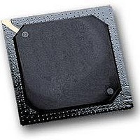
MPC564CZP40 Freescale Semiconductor, MPC564CZP40 Datasheet - Page 117

MPC564CZP40
Manufacturer Part Number
MPC564CZP40
Description
IC MPU 32BIT W/CODE COMP 388PBGA
Manufacturer
Freescale Semiconductor
Series
MPC5xxr
Specifications of MPC564CZP40
Core Processor
PowerPC
Core Size
32-Bit
Speed
40MHz
Connectivity
CAN, EBI/EMI, SCI, SPI, UART/USART
Peripherals
POR, PWM, WDT
Number Of I /o
56
Program Memory Size
512KB (512K x 8)
Program Memory Type
FLASH
Ram Size
32K x 8
Voltage - Supply (vcc/vdd)
2.5 V ~ 2.7 V
Data Converters
A/D 32x10b
Oscillator Type
External
Operating Temperature
-40°C ~ 85°C
Package / Case
388-BGA
Processor Series
MPC5xx
Core
PowerPC
Data Bus Width
32 bit
Data Ram Size
32 KB
Interface Type
CAN, JTAG, QSPI, SCI, SPI, UART
Maximum Clock Frequency
40 MHz
Number Of Programmable I/os
56
Number Of Timers
2
Operating Supply Voltage
0 V to 5 V
Maximum Operating Temperature
+ 85 C
Mounting Style
SMD/SMT
Minimum Operating Temperature
- 40 C
On-chip Adc
2 (10 bit, 32 Channel)
For Use With
MPC564EVB - KIT EVAL FOR MPC561/562/563/564
Lead Free Status / RoHS Status
Contains lead / RoHS non-compliant
Eeprom Size
-
Lead Free Status / Rohs Status
No
Available stocks
Company
Part Number
Manufacturer
Quantity
Price
Company:
Part Number:
MPC564CZP40
Manufacturer:
Freescale Semiconductor
Quantity:
10 000
- Current page: 117 of 1420
- Download datasheet (11Mb)
Freescale Semiconductor
MPIO32B12 / C_CNTX0
MPIO32B13 / PPM_TCLK
MPIO32B14 / PPM_RX0
MPIO32B15 / PPM_TX0
A_TPUCH[0:15]
A_T2CLK / PCS5
B_TPUCH[0:15]
B_T2CLK / PCS4
NVDDL
QVDDL
VDDH
VDD
KAPWR
Signal Name
6
Table 2-1. MPC561/MPC563 Signal Descriptions (continued)
Signals
No. of
16
16
1
1
1
1
1
1
1
1
1
1
1
MPC561/MPC563 Reference Manual, Rev. 1.2
Type
I/O
I/O
I/O
I/O
I/O
I/O
I/O
I/O
O
O
O
O
O
I
I
I
I
I
I
MPIO32B12
MPIO32B13
MPIO32B14
MPIO32B15
A_TPUCH[0:15] Provides TPU module A with 16 input/output programmable
A_T2CLK
B_TPUCH[0:15] Provides TPU module B with 16 input/output programmable
B_T2CLK
NVDDL
QVDDL
VDDH
VDD
KAPWR
Function after
Reset
Global Power
1
TPU
MIOS14 GPIO 12. This function allows the signals to be
used as general-purpose inputs/outputs.
TouCAN_C Transmit Data. This is the serial data output
signal for the TouCAN_C module.
MIOS14 GPIO 13. This function allows the signals to be
used as general-purpose inputs/outputs.
PPM_TCLK. PPM bus clock
MIOS14 GPIO 14. This function allows the signals to be
used as general-purpose inputs/outputs.
PPM_RX0. Receive data to the PPM channel number 0.
MIOS14 GPIO 15. This function allows the signals to be
used as general-purpose inputs/outputs.
PPM_TX0. Transmit data from PPM channel number 0.
timed events.
This signal is used to clock or gate the timer count register
2 (TCR2) within the TPU module A. This signal is an
output-only in special test mode.
PCS5. This signal provides QSPI peripheral chip select
when the enhanced PCS mode is selected.
timed events.
This signal is used to clock or gate the timer count register
2 (TCR2) within the TPU module B. This signal is an
output-only in special test mode.
PCS4. This signal provides QSPI peripheral chip select
when the enhanced PCS mode is selected.
NVDDL. Noisy 2.6-V voltage supply input. This signal
supplies the final output stage of the 2.6-V pad output
drivers. The NVDDL and QVDDL supplies should be
connected to the same power supply in a user's system.
QVDDL. Quiet 2.6-V voltage supply input. This signal
supplies all pad logic and pre-driver circuitry, except for the
final output stage of the 2.6-V pad output drivers.
The NVDDL and QVDDL supplies should be connected to
the same power supply in a user's system.
VDDH. 5-V voltage supply input.
VDD. 2.6-V voltage supply input for internal logic.
Keep-Alive Power. 2.6-V voltage supply input for the
oscillator and keep-alive registers.
Description
Signal Descriptions
2-19
Related parts for MPC564CZP40
Image
Part Number
Description
Manufacturer
Datasheet
Request
R

Part Number:
Description:
MPC5 1K0 5%
Manufacturer:
TE Connectivity
Datasheet:

Part Number:
Description:
MPC5 500R 5%
Manufacturer:
TE Connectivity
Datasheet:

Part Number:
Description:
MPC5 5K0 5%
Manufacturer:
Tyco Electronics
Datasheet:

Part Number:
Description:
MPC5 5R0 5%
Manufacturer:
Tyco Electronics
Datasheet:

Part Number:
Description:
MPC5 50K 5%
Manufacturer:
Tyco Electronics
Datasheet:

Part Number:
Description:
MPC5 1R0 5%
Manufacturer:
Tyco Electronics
Datasheet:
Part Number:
Description:
Manufacturer:
Freescale Semiconductor, Inc
Datasheet:
Part Number:
Description:
Manufacturer:
Freescale Semiconductor, Inc
Datasheet:
Part Number:
Description:
Manufacturer:
Freescale Semiconductor, Inc
Datasheet:
Part Number:
Description:
Manufacturer:
Freescale Semiconductor, Inc
Datasheet:
Part Number:
Description:
Manufacturer:
Freescale Semiconductor, Inc
Datasheet:


