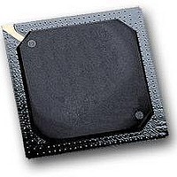
MPC564CZP40 Freescale Semiconductor, MPC564CZP40 Datasheet - Page 864

MPC564CZP40
Manufacturer Part Number
MPC564CZP40
Description
IC MPU 32BIT W/CODE COMP 388PBGA
Manufacturer
Freescale Semiconductor
Series
MPC5xxr
Specifications of MPC564CZP40
Core Processor
PowerPC
Core Size
32-Bit
Speed
40MHz
Connectivity
CAN, EBI/EMI, SCI, SPI, UART/USART
Peripherals
POR, PWM, WDT
Number Of I /o
56
Program Memory Size
512KB (512K x 8)
Program Memory Type
FLASH
Ram Size
32K x 8
Voltage - Supply (vcc/vdd)
2.5 V ~ 2.7 V
Data Converters
A/D 32x10b
Oscillator Type
External
Operating Temperature
-40°C ~ 85°C
Package / Case
388-BGA
Processor Series
MPC5xx
Core
PowerPC
Data Bus Width
32 bit
Data Ram Size
32 KB
Interface Type
CAN, JTAG, QSPI, SCI, SPI, UART
Maximum Clock Frequency
40 MHz
Number Of Programmable I/os
56
Number Of Timers
2
Operating Supply Voltage
0 V to 5 V
Maximum Operating Temperature
+ 85 C
Mounting Style
SMD/SMT
Minimum Operating Temperature
- 40 C
On-chip Adc
2 (10 bit, 32 Channel)
For Use With
MPC564EVB - KIT EVAL FOR MPC561/562/563/564
Lead Free Status / RoHS Status
Contains lead / RoHS non-compliant
Eeprom Size
-
Lead Free Status / Rohs Status
No
Available stocks
Company
Part Number
Manufacturer
Quantity
Price
Company:
Part Number:
MPC564CZP40
Manufacturer:
Freescale Semiconductor
Quantity:
10 000
- Current page: 864 of 1420
- Download datasheet (11Mb)
CDR3 Flash (UC3F) EEPROM
The UC3F EEPROM module array is divided into array blocks to allow for independent erase, address
attributes restrictions, and protection from program and erase for each array block. The size of a large array
block in the UC3F module is fixed at 64 Kbytes. The size of a subdivided large block becomes the original
large array block size minus 16 Kbytes (64 Kbytes – 16 Kbytes = 48 Kbytes). The size of the small block,
which is the remainder of the large block, is always 16 Kbytes. The total UC3F EEPROM array is
distributed into eight large blocks, two of which contain small blocks. Information is transferred to the
UC3F EEPROM by long-word (64 bits), word (32 bits), half-word (16 bits), or byte (8 bits).
To improve system performance, each array read access retrieves 32 bytes of information. These 32 bytes
may be copied into one of two read page buffers aligned to the low order addresses. The two read page
buffers are independently updated by page management logic contained in the BIU which interfaces to the
UC3F EEPROM module.
21-2
B0EPEE
VFLASH
EPEE
VDDF
VSSF
U-Bus
Figure 21-1. Block Diagram for a 512 Kbyte UC3F Module Configuration
Memory Interface (MI)
Internal
Timer
MPC561/MPC563 Reference Manual, Rev. 1.2
Program/Erase
Read Control
Program/Erase
Control
Generation
Voltage
Bus Interface Unit (BIU)
UC3F Array Core
Register
Block
Pgm Data
Block 0 (16 Kbytes + 48 Kbytes)
Block 1 (48 Kbytes + 16 Kbytes)
Block 2 (64 Kbytes)
Block 3 (64 Kbytes)
Block 4 (64 Kbytes)
Block 5 (64 Kbytes)
Block 6 (64 Kbytes)
Block 7 (64 Kbytes)
Latch
Column Decode
Data Mux
Read Page Buffer 0
Read Page Buffer 1
Freescale Semiconductor
Related parts for MPC564CZP40
Image
Part Number
Description
Manufacturer
Datasheet
Request
R

Part Number:
Description:
MPC5 1K0 5%
Manufacturer:
TE Connectivity
Datasheet:

Part Number:
Description:
MPC5 500R 5%
Manufacturer:
TE Connectivity
Datasheet:

Part Number:
Description:
MPC5 5K0 5%
Manufacturer:
Tyco Electronics
Datasheet:

Part Number:
Description:
MPC5 5R0 5%
Manufacturer:
Tyco Electronics
Datasheet:

Part Number:
Description:
MPC5 50K 5%
Manufacturer:
Tyco Electronics
Datasheet:

Part Number:
Description:
MPC5 1R0 5%
Manufacturer:
Tyco Electronics
Datasheet:
Part Number:
Description:
Manufacturer:
Freescale Semiconductor, Inc
Datasheet:
Part Number:
Description:
Manufacturer:
Freescale Semiconductor, Inc
Datasheet:
Part Number:
Description:
Manufacturer:
Freescale Semiconductor, Inc
Datasheet:
Part Number:
Description:
Manufacturer:
Freescale Semiconductor, Inc
Datasheet:
Part Number:
Description:
Manufacturer:
Freescale Semiconductor, Inc
Datasheet:


