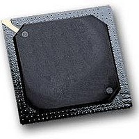
MPC564CZP40 Freescale Semiconductor, MPC564CZP40 Datasheet - Page 608

MPC564CZP40
Manufacturer Part Number
MPC564CZP40
Description
IC MPU 32BIT W/CODE COMP 388PBGA
Manufacturer
Freescale Semiconductor
Series
MPC5xxr
Specifications of MPC564CZP40
Core Processor
PowerPC
Core Size
32-Bit
Speed
40MHz
Connectivity
CAN, EBI/EMI, SCI, SPI, UART/USART
Peripherals
POR, PWM, WDT
Number Of I /o
56
Program Memory Size
512KB (512K x 8)
Program Memory Type
FLASH
Ram Size
32K x 8
Voltage - Supply (vcc/vdd)
2.5 V ~ 2.7 V
Data Converters
A/D 32x10b
Oscillator Type
External
Operating Temperature
-40°C ~ 85°C
Package / Case
388-BGA
Processor Series
MPC5xx
Core
PowerPC
Data Bus Width
32 bit
Data Ram Size
32 KB
Interface Type
CAN, JTAG, QSPI, SCI, SPI, UART
Maximum Clock Frequency
40 MHz
Number Of Programmable I/os
56
Number Of Timers
2
Operating Supply Voltage
0 V to 5 V
Maximum Operating Temperature
+ 85 C
Mounting Style
SMD/SMT
Minimum Operating Temperature
- 40 C
On-chip Adc
2 (10 bit, 32 Channel)
For Use With
MPC564EVB - KIT EVAL FOR MPC561/562/563/564
Lead Free Status / RoHS Status
Contains lead / RoHS non-compliant
Eeprom Size
-
Lead Free Status / Rohs Status
No
Available stocks
Company
Part Number
Manufacturer
Quantity
Price
Company:
Part Number:
MPC564CZP40
Manufacturer:
Freescale Semiconductor
Quantity:
10 000
- Current page: 608 of 1420
- Download datasheet (11Mb)
QADC64E Enhanced Mode Operation
Each port A or B signal is configured as an input or output by programming the port data direction register
(DDRQA or DDRQB). The digital input signal states are read by the software in the upper half of the port
data register when the port data direction register specifies that the signals are inputs. The digital data in
the port data register is driven onto the port A or B signals when the corresponding bit in the port data
direction register specifies output. Refer to
Since the outputs are configured as push-pull drivers, external pull-up provisions are not necessary when
the output is used to drive another integrated circuit.
14.6.2
The QADC64E uses two external trigger signals (ETRIG[2:1]). Each of the two input external trigger
signals is associated with one of the scan queues, queue 1 or queue 2 The assignment of ETRIG[2:1] to a
queue is made in the QACR0 register by the TRG bit. When TRG=0, ETRIG1 triggers queue 1 and
ETRIG2 triggers queue 2. When TRG=1, ETRIG1 triggers queue 2 and ETRIG2 triggers queue 1.
14.6.3
V
power is required to isolate the sensitive analog circuitry from the normal levels of noise present on the
digital power supply. Refer to
The analog supply signals (V
V
14-66
DDA
RL
) and of the analog multiplexer inputs.
16 CHANNELS
and V
External Trigger Input Signals
Analog Power Signals
SSA
signals supply power to the analog subsystems of the QADC64E module. Dedicated
DDA
Figure 14-47. Equivalent Analog Input Circuitry
Appendix F, “Electrical
MPC561/MPC563 Reference Manual, Rev. 1.2
and V
SSA
) define the limits of the analog reference voltages (V
Figure 14-47
C
Appendix B, “Internal Memory
SAMPLE
P
AMP
V
V
DDA
SSA
Characteristics,” for more information.
is a diagram of the analog input circuitry.
S/H
RC DAC
Comparator
V
RH
V
RL
QADC64E 16CH SAMPLE AMP
Map” for more information.
Freescale Semiconductor
RH
and
Related parts for MPC564CZP40
Image
Part Number
Description
Manufacturer
Datasheet
Request
R

Part Number:
Description:
MPC5 1K0 5%
Manufacturer:
TE Connectivity
Datasheet:

Part Number:
Description:
MPC5 500R 5%
Manufacturer:
TE Connectivity
Datasheet:

Part Number:
Description:
MPC5 5K0 5%
Manufacturer:
Tyco Electronics
Datasheet:

Part Number:
Description:
MPC5 5R0 5%
Manufacturer:
Tyco Electronics
Datasheet:

Part Number:
Description:
MPC5 50K 5%
Manufacturer:
Tyco Electronics
Datasheet:

Part Number:
Description:
MPC5 1R0 5%
Manufacturer:
Tyco Electronics
Datasheet:
Part Number:
Description:
Manufacturer:
Freescale Semiconductor, Inc
Datasheet:
Part Number:
Description:
Manufacturer:
Freescale Semiconductor, Inc
Datasheet:
Part Number:
Description:
Manufacturer:
Freescale Semiconductor, Inc
Datasheet:
Part Number:
Description:
Manufacturer:
Freescale Semiconductor, Inc
Datasheet:
Part Number:
Description:
Manufacturer:
Freescale Semiconductor, Inc
Datasheet:


