MPC564CZP40 Freescale Semiconductor, MPC564CZP40 Datasheet - Page 846
MPC564CZP40
Manufacturer Part Number
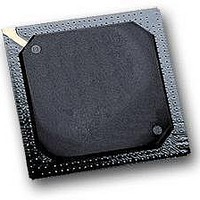
MPC564CZP40
Description
IC MPU 32BIT W/CODE COMP 388PBGA
Manufacturer
Freescale Semiconductor
Series
MPC5xxr
Specifications of MPC564CZP40
Core Processor
PowerPC
Core Size
32-Bit
Speed
40MHz
Connectivity
CAN, EBI/EMI, SCI, SPI, UART/USART
Peripherals
POR, PWM, WDT
Number Of I /o
56
Program Memory Size
512KB (512K x 8)
Program Memory Type
FLASH
Ram Size
32K x 8
Voltage - Supply (vcc/vdd)
2.5 V ~ 2.7 V
Data Converters
A/D 32x10b
Oscillator Type
External
Operating Temperature
-40°C ~ 85°C
Package / Case
388-BGA
Processor Series
MPC5xx
Core
PowerPC
Data Bus Width
32 bit
Data Ram Size
32 KB
Interface Type
CAN, JTAG, QSPI, SCI, SPI, UART
Maximum Clock Frequency
40 MHz
Number Of Programmable I/os
56
Number Of Timers
2
Operating Supply Voltage
0 V to 5 V
Maximum Operating Temperature
+ 85 C
Mounting Style
SMD/SMT
Minimum Operating Temperature
- 40 C
On-chip Adc
2 (10 bit, 32 Channel)
For Use With
MPC564EVB - KIT EVAL FOR MPC561/562/563/564
Lead Free Status / RoHS Status
Contains lead / RoHS non-compliant
Eeprom Size
-
Lead Free Status / Rohs Status
No
Available stocks
Company
Part Number
Manufacturer
Quantity
Price
Company:

Part Number:
MPC564CZP40
Manufacturer:
Freescale Semiconductor
Quantity:
10 000


Time Processor Unit 3
19.4.7
The host sequence field selects the mode of operation for the time function selected on a given channel.
The meaning of the host sequence bits depends on the time function specified. See
ROM
19-16
SRESET
SRESET
SRESET
SRESET
Field
Addr
Field
Addr
Functions,” for definitions of the host service request bits for the predefined TPU ROM functions.
Field
Field
Addr
Addr
CH[15:0]
Name
MSB
MSB
0
Host Sequence Registers (HSQRn)
MSB
MSB
0
0
0
1
1
CH 7
1
1
Encoded time function for each channel. Encoded four-bit fields in the channel function select
registers specify one of 16 time functions to be executed on the corresponding channel.
CH 3
CH 15
CH 11
Figure 19-10. CFSR0 — Channel Function Select Register 0
Figure 19-11. CFSR1 — Channel Function Select Register 1
Figure 19-12. CFSR2 — Channel Function Select Register 2
Figure 19-13. CFSR3 — Channel Function Select Register 3
2
2
2
2
3
3
3
3
MPC561/MPC563 Reference Manual, Rev. 1.2
Table 19-12. CFSRn Bit Descriptions
4
4
4
4
0x30 400C (TPU_A), 0x30 440C (TPU_B)
0x30 400E (TPU_A), 0x30 440E (TPU_B)
0x30 4010 (TPU_A), 0x30 4410 (TPU_B)
0x30 4012 (TPU_A), 0x30 4412 (TPU_B)
5
5
5
5
CH 14
CH 10
CH 6
CH 2
0000_0000_0000_0000
0000_0000_0000_0000
0000_0000_0000_0000
0000_0000_0000_0000
6
6
6
6
7
7
7
7
Description
8
8
8
8
9
9
9
9
CH 13
CH 9
CH 1
CH 5
10
10
10
10
11
11
11
11
12
12
12
12
Appendix D, “TPU3
Freescale Semiconductor
13
13
13
CH 12
13
CH 8
CH 0
CH 4
14
14
14
14
LSB
LSB
15
15
LSB
15
LSB
15
Related parts for MPC564CZP40
Image
Part Number
Description
Manufacturer
Datasheet
Request
R

Part Number:
Description:
MPC5 1K0 5%
Manufacturer:
TE Connectivity
Datasheet:


Part Number:
Description:
MPC5 500R 5%
Manufacturer:
TE Connectivity
Datasheet:

Part Number:
Description:
MPC5 5K0 5%
Manufacturer:
Tyco Electronics
Datasheet:
Part Number:
Description:
MPC5 5R0 5%
Manufacturer:
Tyco Electronics
Datasheet:
Part Number:
Description:
MPC5 50K 5%
Manufacturer:
Tyco Electronics
Datasheet:
Part Number:
Description:
MPC5 1R0 5%
Manufacturer:
Tyco Electronics
Datasheet:

Part Number:
Description:
Manufacturer:
Freescale Semiconductor, Inc
Datasheet:
Part Number:
Description:
Manufacturer:
Freescale Semiconductor, Inc
Datasheet:
Part Number:
Description:
Manufacturer:
Freescale Semiconductor, Inc
Datasheet:
Part Number:
Description:
Manufacturer:
Freescale Semiconductor, Inc
Datasheet:
Part Number:
Description:
Manufacturer:
Freescale Semiconductor, Inc
Datasheet: