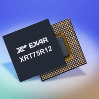
XRT75R12DIB-F Exar Corporation, XRT75R12DIB-F Datasheet - Page 123

XRT75R12DIB-F
Manufacturer Part Number
XRT75R12DIB-F
Description
Peripheral Drivers & Components (PCIs) 12 Channel 3.3V-5V temp -45 to 85C
Manufacturer
Exar Corporation
Datasheet
1.XRT75R12DIB-F.pdf
(133 pages)
Specifications of XRT75R12DIB-F
Maximum Operating Temperature
+ 85 C
Minimum Operating Temperature
- 40 C
Mounting Style
SMD/SMT
Operating Supply Voltage
3.3 V to 5 V
Package / Case
TBGA-420
Lead Free Status / RoHS Status
Lead free / RoHS Compliant
- Current page: 123 of 133
- Download datasheet (851Kb)
REV. 1.0.3
N
In order to minimize the effects of "Clock-Gapping" Jitter within the DS3 signal that is ultimately transmitted to
the DS3 Line (or facility), we recommend that some "pre-processing" of the "Data-Signals" and "Clock-Signals"
(which are output from the Mapper device) be implemented prior to routing these signals to the "Transmit
Inputs" of the LIU.
Our simulation results indicate that Jitter Attenuator PLL (within the LIU LIU IC) will have no problem handling
and processing the "Data-Signal" and "Clock-Signal" from a Mapper IC/ASIC if no pre-processing has been
performed on these signals. In order words, our simulation results indicate that the Jitter Attenuator PLL
(within the LIU IC) will have no problem handling the "worst-case" of 59 consecutive bits of no clock pulses in
the "Clock-Signal (due to the Mapper IC processing the TOH bytes, an Incrementing Pointer-Adjustment-
induced "stuffed-byte", the POH byte, and the two fixed-stuff bytes within the STS-1 SPE, etc), immediately
followed be processing clusters of DS3 data-bits (as shown in
Intrinsic Jitter Requirements per Telcordia GR-253-CORE for DS3 applications.
N
For the time-being, we recommend that the customer implement the "pre-processing" of the DS3 "Data-Signal"
and "Clock-Signal" as described below. Currently we are aware that some of the Mapper products on the
Market do implement this exact "pre-processing" algorithm. However, if the customer is implementing their
Mapper Design in an ASIC or FPGA solution, then we strongly recommend that the user implement the
necessary logic design to realize the following recommendations.
Some time ago, we spent some time, studying (and then later testing our solution with) the PM5342 OC-3 to
DS3 Mapper IC from PMC-Sierra. In particular, we wanted to understand the type of "DS3 Clock" and "Data"
signal that this DS3 to OC-3 Mapper IC outputs.
8.8.2
8.8.2.1
8.8.2.2
OTES
OTE
1. The ability to disable the "SONET APS Recovery Time" mode is optional.
2. The "SONET APS Recovery Time" mode will be discussed in greater detail in
B
: If this sort of "pre-processing" is already supported by the Mapper device that you are using, then no further action
R/O
:
IT
0
is required by the user.
7
LIU permit the user to comply with the SONET APS Recovery Time requirements of 50ms (per
Telcordia GR-253-CORE)?” on page 123
T
ABLE
Recommendations on Pre-Processing the Gapped Clocks (from the Mapper/ASIC Device)
prior to routing this DS3 Clock and Data-Signals to the Transmit Inputs of the LIU
TWELVE CHANNEL E3/DS3/STS-1 LINE INTERFACE UNIT WITH SONET DESYNCHRONIZER
SOME NOTES PRIOR TO STARTING THIS DISCUSSION:
OUR PRE-PROCESSING RECOMMENDATIONS
49: J
Unused
B
R/O
IT
0
ITTER
6
A
TTENUATOR
B
R/O
IT
0
5
C
ONTROL
SONET APS
DisableCh_n
(
M
Recovery
= 0-5 & 8-D) (
B
Time
R/W
IT
0
4
R
.
EGISTER
119
JA RESET
N
= [0:11])
B
Ch_n
R/W
- C
IT
0
Figure
3
HANNEL N
44) and still comply with the "Category I
JA1 Ch_n
, A
B
R/W
IT
0
DDRESS
2
“Section 8.8.3, How does the
JA in Tx Path
L
OCATION
Ch_n
B
R/W
IT
0
1
XRT75R12D
; 0
XM
JA0 Ch_n
7
B
R/W
IT
1
0
Related parts for XRT75R12DIB-F
Image
Part Number
Description
Manufacturer
Datasheet
Request
R

Part Number:
Description:
Twelve Channel E3/ds3/sts-1 Line Interface Unit With Jitter
Manufacturer:
Exar Corporation
Datasheet:

Part Number:
Description:
BiCMOS Fixed, Quad, Voltage Output, Single or Dual Supply 8-Bit Digital-to-Analog Converter
Manufacturer:
Exar Corporation
Datasheet:

Part Number:
Description:
Manufacturer:
Exar Corporation
Datasheet:

Part Number:
Description:
Voltage-Controlled Oscillator
Manufacturer:
Exar Corporation
Datasheet:

Part Number:
Description:
INTEGRATED LINE TRANSMITTER
Manufacturer:
Exar Corporation
Datasheet:

Part Number:
Description:
Monolithic Function Generator
Manufacturer:
Exar Corporation
Datasheet:

Part Number:
Description:
CMOS Microprocessor Compatible Double-Buffered 12-Bit Digital-to-Analog Converter
Manufacturer:
Exar Corporation
Datasheet:

Part Number:
Description:
CMOS 6 BIT HIGH SPEED ANALOG TO DIGITAL CONVERTER
Manufacturer:
Exar Corporation
Datasheet:

Part Number:
Description:
Manufacturer:
Exar Corporation
Datasheet:

Part Number:
Description:
Manufacturer:
Exar Corporation
Datasheet:

Part Number:
Description:
8-Channel, Voltage Output 10 MHz Input Bandwidth 8-Bit Multiplying DACs with Serial Digital Data Por
Manufacturer:
Exar Corporation
Datasheet:

Part Number:
Description:
15 V CMOS Multiplying10-Bit Digital-to-Analog Converter
Manufacturer:
Exar Corporation
Datasheet:

Part Number:
Description:
Monolithic Function Generator
Manufacturer:
Exar Corporation
Datasheet:


