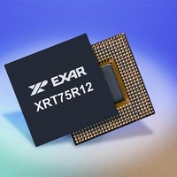
XRT75R12DIB-F Exar Corporation, XRT75R12DIB-F Datasheet - Page 51

XRT75R12DIB-F
Manufacturer Part Number
XRT75R12DIB-F
Description
Peripheral Drivers & Components (PCIs) 12 Channel 3.3V-5V temp -45 to 85C
Manufacturer
Exar Corporation
Datasheet
1.XRT75R12DIB-F.pdf
(133 pages)
Specifications of XRT75R12DIB-F
Maximum Operating Temperature
+ 85 C
Minimum Operating Temperature
- 40 C
Mounting Style
SMD/SMT
Operating Supply Voltage
3.3 V to 5 V
Package / Case
TBGA-420
Lead Free Status / RoHS Status
Lead free / RoHS Compliant
- Current page: 51 of 133
- Download datasheet (851Kb)
REV. 1.0.3
Whether the LIU is configured for Asynchronous or Synchronous mode, the following descriptions apply. The
synchronous mode requires an input clock (PCLK) to be used as the microprocessor timing reference. Read
and Write operations are described below.
Read Cycle (For Pmode = "0" or "1")
Whenever the local µP wishes to read the contents of a register, it should do the following.
Write Cycle (For Pmode = "0" or "1")
Whenever a local µP wishes to write a byte or word of data into a register within the LIU, it should do the follow-
ing.
F
1. Place the address of the target register on the address bus input pins Addr[7:0].
2. While the µP is placing this address value on the address bus, the address decoding circuitry should
3. Next, the µP should indicate that this current bus cycle is a Read operation by toggling the RD input pin
4. After the µP toggles the Read signal "Low", the LIU will toggle the RDY output pin "Low". The LIU does this
5. After the µP detects the RDY signal and has read the data, it can terminate the Read Cycle by toggling the
6. The CS input pin must be pulled "High" before a new command can be issued.
1. Place the address of the target register on the address bus input pins Addr[7:0].
2. While the µP is placing this address value on the address bus, the address decoding circuitry should
3. The µP should then place the byte or word that it intends to write into the target register, on the bi-direc-
4. Next, the µP should indicate that this current bus cycle is a Write operation by toggling the
5. After the µP toggles the Write signal "Low", the LIU will toggle the RDY output pin "Low". The LIU does this
6. The CS input pin must be pulled "High" before a new command can be issued.
7.2 A
IGURE
assert the CS pin of the LIU, by toggling it "Low". This action enables communication between the µP and
the LIU microprocessor interface block.
"Low". This action enables the bi-directional data bus output drivers of the LIU.
to inform the µP that the data is available to be read by the µP, and that it is ready for the next command.
RD input pin "High".
assert the CS pin of the LIU, by toggling it "Low". This action enables communication between the µP and
the LIU microprocessor interface block.
tional data bus D[7:0].
"Low". This action enables the bi-directional data bus input drivers of the LIU.
to inform the µP that the data has been written into the internal register location, and that it is ready for the
next command.
Addr[7:0]
SYNCHRONOUS AND
35. A
RDY
D[7:0]
WR
RD
CS
TWELVE CHANNEL E3/DS3/STS-1 LINE INTERFACE UNIT WITH SONET DESYNCHRONIZER
SYNCHRONOUS
t
0
t
1
S
YNCHRONOUS
µP I
Valid Address
READ OPERATION
NTERFACE
t
2
D
Valid Data for Readback
S
ESCRIPTION
IGNALS
D
47
URING
P
ROGRAMMED
t
0
t
3
I/O R
Data Available to Write Into the LIU
WRITE OPERATION
t
4
EAD AND
Valid Address
W
RITE
XRT75R12D
O
WR
PERATIONS
input pin
Related parts for XRT75R12DIB-F
Image
Part Number
Description
Manufacturer
Datasheet
Request
R

Part Number:
Description:
Twelve Channel E3/ds3/sts-1 Line Interface Unit With Jitter
Manufacturer:
Exar Corporation
Datasheet:

Part Number:
Description:
BiCMOS Fixed, Quad, Voltage Output, Single or Dual Supply 8-Bit Digital-to-Analog Converter
Manufacturer:
Exar Corporation
Datasheet:

Part Number:
Description:
Manufacturer:
Exar Corporation
Datasheet:

Part Number:
Description:
Voltage-Controlled Oscillator
Manufacturer:
Exar Corporation
Datasheet:

Part Number:
Description:
INTEGRATED LINE TRANSMITTER
Manufacturer:
Exar Corporation
Datasheet:

Part Number:
Description:
Monolithic Function Generator
Manufacturer:
Exar Corporation
Datasheet:

Part Number:
Description:
CMOS Microprocessor Compatible Double-Buffered 12-Bit Digital-to-Analog Converter
Manufacturer:
Exar Corporation
Datasheet:

Part Number:
Description:
CMOS 6 BIT HIGH SPEED ANALOG TO DIGITAL CONVERTER
Manufacturer:
Exar Corporation
Datasheet:

Part Number:
Description:
Manufacturer:
Exar Corporation
Datasheet:

Part Number:
Description:
Manufacturer:
Exar Corporation
Datasheet:

Part Number:
Description:
8-Channel, Voltage Output 10 MHz Input Bandwidth 8-Bit Multiplying DACs with Serial Digital Data Por
Manufacturer:
Exar Corporation
Datasheet:

Part Number:
Description:
15 V CMOS Multiplying10-Bit Digital-to-Analog Converter
Manufacturer:
Exar Corporation
Datasheet:

Part Number:
Description:
Monolithic Function Generator
Manufacturer:
Exar Corporation
Datasheet:


