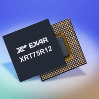
XRT75R12DIB-F Exar Corporation, XRT75R12DIB-F Datasheet - Page 87

XRT75R12DIB-F
Manufacturer Part Number
XRT75R12DIB-F
Description
Peripheral Drivers & Components (PCIs) 12 Channel 3.3V-5V temp -45 to 85C
Manufacturer
Exar Corporation
Datasheet
1.XRT75R12DIB-F.pdf
(133 pages)
Specifications of XRT75R12DIB-F
Maximum Operating Temperature
+ 85 C
Minimum Operating Temperature
- 40 C
Mounting Style
SMD/SMT
Operating Supply Voltage
3.3 V to 5 V
Package / Case
TBGA-420
Lead Free Status / RoHS Status
Lead free / RoHS Compliant
- Current page: 87 of 133
- Download datasheet (851Kb)
REV. 1.0.3
J
T
ITTER
B
ABLE
IT
7 - 4
B
N
IT
UMBER
3
2
1
0
36: XRT75R12D R
A
7
TTENUATOR
TWELVE CHANNEL E3/DS3/STS-1 LINE INTERFACE UNIT WITH SONET DESYNCHRONIZER
JA in Tx Path Ch_n
JA RESET Ch_n
B
JA1 Ch_n
JA0 Ch_n
Reserved
IT
C
N
6
AME
ONTROL
Reserved
EGISTER
R
B
EGISTER
IT
MAP
T
R/W
R/W
R/W
R/W
5
YPE
SHOWING
- C
Jitter Attenuator RESET - Channel_n:
Writing a "0 to 1" transition within this bit-field will configure the Jitter Attenu-
ator (within Channel_n) to execute a RESET operation.
Whenever the user executes a RESET operation, then following will occur.
•
•
N
Jitter Attenuator Configuration Select Input - Bit 1:
This READ/WRITE bit-field, along with Bit 0 (JA0 Ch_n) is used to do any of
the following.
•
•
The relationship between the settings of these two bit-fields and the Enable/
Disable States, and FIFO Depths is presented below.
Jitter Attenuator in Transmit/Receive Path Select Bit:
This input pin is used to configure the Jitter Attenuator (within Channel_n) to
operate in either the Transmit or Receive path, as described below.
0 - Configures the Jitter Attenuator (within Channel_n) to operate in the
Receive Path.
1 - Configures the Jitter Attenuator (within Channel_n) to operate in the
Transmit Path.
Jitter Attenuator Configuration Select Input - Bit 0:
See the description for Bit 2 (JA1 Ch_n).
OTE
The READ and WRITE pointers (within the Jitter Attenuator FIFO) will be
reset to their default values.
The contents of the Jitter Attenuator FIFO will be flushed.
To enable or disable the Jitter Attenuator corresponding to Channel_n.
To select the FIFO Depth for the Jitter Attenuator within Channel_n.
HANNEL N
B
: The user must follow up any "0 to 1" transition with the appropriate
IT
write operate to set this bit-field back to "0", in order to resume
normal operation with the Jitter Attenuator.
4
J
ITTER
A
JA0
83
0
0
1
1
DDRESS
A
JA RESET
TTENUATOR
B
Ch_n
R/W
JA1
IT
0
1
0
1
3
L
OCATION
SONET/SDH De-Sync Mode
D
C
Jitter Attenuator Mode
JA1 Ch_n
ESCRIPTION
ONTROL
FIFO Depth = 16 bits
FIFO Depth = 32 bits
B
R/W
= 0
IT
2
XM
Disabled
7 (
R
EGISTERS
M
JA in Tx Path
= 0-5 & 8-D)
Ch_n
B
R/W
IT
1
(JA_
XRT75R12D
N
)
JA0 Ch_n
(
N
B
R/W
= [0:11])
IT
0
Related parts for XRT75R12DIB-F
Image
Part Number
Description
Manufacturer
Datasheet
Request
R

Part Number:
Description:
Twelve Channel E3/ds3/sts-1 Line Interface Unit With Jitter
Manufacturer:
Exar Corporation
Datasheet:

Part Number:
Description:
BiCMOS Fixed, Quad, Voltage Output, Single or Dual Supply 8-Bit Digital-to-Analog Converter
Manufacturer:
Exar Corporation
Datasheet:

Part Number:
Description:
Manufacturer:
Exar Corporation
Datasheet:

Part Number:
Description:
Voltage-Controlled Oscillator
Manufacturer:
Exar Corporation
Datasheet:

Part Number:
Description:
INTEGRATED LINE TRANSMITTER
Manufacturer:
Exar Corporation
Datasheet:

Part Number:
Description:
Monolithic Function Generator
Manufacturer:
Exar Corporation
Datasheet:

Part Number:
Description:
CMOS Microprocessor Compatible Double-Buffered 12-Bit Digital-to-Analog Converter
Manufacturer:
Exar Corporation
Datasheet:

Part Number:
Description:
CMOS 6 BIT HIGH SPEED ANALOG TO DIGITAL CONVERTER
Manufacturer:
Exar Corporation
Datasheet:

Part Number:
Description:
Manufacturer:
Exar Corporation
Datasheet:

Part Number:
Description:
Manufacturer:
Exar Corporation
Datasheet:

Part Number:
Description:
8-Channel, Voltage Output 10 MHz Input Bandwidth 8-Bit Multiplying DACs with Serial Digital Data Por
Manufacturer:
Exar Corporation
Datasheet:

Part Number:
Description:
15 V CMOS Multiplying10-Bit Digital-to-Analog Converter
Manufacturer:
Exar Corporation
Datasheet:

Part Number:
Description:
Monolithic Function Generator
Manufacturer:
Exar Corporation
Datasheet:


