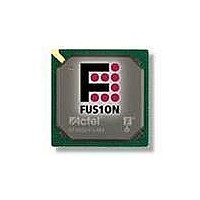
AFS250-FGG256 Actel, AFS250-FGG256 Datasheet - Page 154

AFS250-FGG256
Manufacturer Part Number
AFS250-FGG256
Description
FPGA - Field Programmable Gate Array 250K System Gates
Manufacturer
Actel
Datasheet
1.AFS600-PQG208.pdf
(330 pages)
Specifications of AFS250-FGG256
Processor Series
AFS250
Core
IP Core
Maximum Operating Frequency
1098.9 MHz
Number Of Programmable I/os
114
Data Ram Size
36864
Supply Voltage (max)
1.575 V
Maximum Operating Temperature
+ 70 C
Minimum Operating Temperature
0 C
Development Tools By Supplier
AFS-Eval-Kit, AFS-BRD600, FlashPro 3, FlashPro Lite, Silicon-Explorer II, Silicon-Sculptor 3, SI-EX-TCA
Mounting Style
SMD/SMT
Supply Voltage (min)
1.425 V
Number Of Gates
250 K
Package / Case
FPBGA-256
Lead Free Status / RoHS Status
Lead free / RoHS Compliant
Available stocks
Company
Part Number
Manufacturer
Quantity
Price
Company:
Part Number:
AFS250-FGG256
Manufacturer:
Actel
Quantity:
135
Company:
Part Number:
AFS250-FGG256
Manufacturer:
ACTEL
Quantity:
6 800
Company:
Part Number:
AFS250-FGG256I
Manufacturer:
Microsemi SoC
Quantity:
10 000
- Current page: 154 of 330
- Download datasheet (13Mb)
Device Architecture
Table 2-69 • Fusion Pro I/O Features
2- 13 8
Feature
Single-ended
referenced transmitter
features
Single-ended receiver features
Voltage-referenced
receiver features
CMOS-style
M-LVDS, or LVPECL
transmitter
LVDS/LVPECL differential
receiver features
Features Supported on Pro I/Os
Table 2-69
LVDS,
and
differential
lists all features supported by transmitter/receiver for single-ended and differential I/Os.
voltage-
BLVDS,
•
•
•
•
•
•
•
•
•
•
•
•
•
•
•
•
•
•
•
•
•
•
•
•
•
Hot insertion in every mode except PCI or 5 V input tolerant (these modes use
clamp diodes and do not allow hot insertion)
Activation of hot insertion (disabling the clamp diode) is selectable by I/Os.
Weak pull-up and pull-down
Two slew rates
Skew between output buffer enable/disable time: 2 ns delay (rising edge) and
0 ns delay (falling edge); see
Enable/Disable Time" on page 2-151
Five drive strengths
5 V–tolerant receiver
LVTTL/LVCMOS 3.3 V outputs compatible with 5 V TTL inputs
Tolerance" section on page
High performance
Schmitt trigger option
ESD protection
Programmable delay: 0 ns if bypassed, 0.625 ns with '000' setting, 6.575 ns
with '111' setting, 0.85-ns intermediate delay increments (at 25°C, 1.5 V)
High performance
Separate ground planes, GND/GNDQ, for input buffers only to avoid output-
induced noise in the input circuitry
Programmable Delay: 0 ns if bypassed, 0.625 ns with '000' setting, 6.575 ns
with '111' setting, 0.85-ns intermediate delay increments (at 25°C, 1.5 V)
High performance
Separate ground planes, GND/GNDQ, for input buffers only to avoid output-
induced noise in the input circuitry
Two I/Os and external resistors are used to provide a CMOS-style LVDS,
BLVDS, M-LVDS, or LVPECL transmitter solution.
Activation of hot insertion (disabling the clamp diode) is selectable by I/Os.
Weak pull-up and pull-down
Fast slew rate
ESD protection
High performance
Programmable delay: 0.625 ns with '000' setting, 6.575 ns with '111' setting,
0.85-ns intermediate delay increments (at 25°C, 1.5 V)
Separate input buffer ground and power planes to avoid output-induced noise
in the input circuitry
(Table 2-73 on page
(Table 2-73 on page
(Table 2-73 on page
(Table 2-73 on page
R e visio n 1
("5 V Input Tolerance" section on page
2-150)
Description
"Selectable Skew between Output Buffer
for more information
2-145)
2-145)
2-145)
2-145)
2-146)
("5 V Output
Related parts for AFS250-FGG256
Image
Part Number
Description
Manufacturer
Datasheet
Request
R

Part Number:
Description:
FPGA 256/I�/Fusion Voltage: 1.5, 1.8, 2.5, 3.3 Mixed Voltage
Manufacturer:
Actel
Datasheet:

Part Number:
Description:
FPGA - Field Programmable Gate Array 250K System Gates
Manufacturer:
Actel
Datasheet:

Part Number:
Description:
MCU, MPU & DSP Development Tools Silicon Sculptor Programming Mod
Manufacturer:
Actel

Part Number:
Description:
MCU, MPU & DSP Development Tools InSystem Programming ProASICPLUS Devices
Manufacturer:
Actel

Part Number:
Description:
Programming Socket Adapters & Emulators PQ160 Module
Manufacturer:
Actel

Part Number:
Description:
Programming Socket Adapters & Emulators Axcelerator Adap Module Kit
Manufacturer:
Actel

Part Number:
Description:
Programming Socket Adapters & Emulators Evaluation
Manufacturer:
Actel

Part Number:
Description:
Programming Socket Adapters & Emulators AFDX Solutions
Manufacturer:
Actel

Part Number:
Description:
Programming Socket Adapters & Emulators SILICON SCULPTOR ADAPTER MODULE
Manufacturer:
Actel
Datasheet:

Part Number:
Description:
Programming Socket Adapters & Emulators Axcelerator Adap Module Kit
Manufacturer:
Actel

Part Number:
Description:
Programming Socket Adapters & Emulators Evaluation
Manufacturer:
Actel

Part Number:
Description:
Programming Socket Adapters & Emulators Silicon Sculptor Software
Manufacturer:
Actel

Part Number:
Description:
Programming Socket Adapters & Emulators InSystem Programming ProASICPLUS Devices
Manufacturer:
Actel


