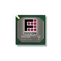
AFS250-FGG256 Actel, AFS250-FGG256 Datasheet - Page 70

AFS250-FGG256
Manufacturer Part Number
AFS250-FGG256
Description
FPGA - Field Programmable Gate Array 250K System Gates
Manufacturer
Actel
Datasheet
1.AFS600-PQG208.pdf
(330 pages)
Specifications of AFS250-FGG256
Processor Series
AFS250
Core
IP Core
Maximum Operating Frequency
1098.9 MHz
Number Of Programmable I/os
114
Data Ram Size
36864
Supply Voltage (max)
1.575 V
Maximum Operating Temperature
+ 70 C
Minimum Operating Temperature
0 C
Development Tools By Supplier
AFS-Eval-Kit, AFS-BRD600, FlashPro 3, FlashPro Lite, Silicon-Explorer II, Silicon-Sculptor 3, SI-EX-TCA
Mounting Style
SMD/SMT
Supply Voltage (min)
1.425 V
Number Of Gates
250 K
Package / Case
FPBGA-256
Lead Free Status / RoHS Status
Lead free / RoHS Compliant
Available stocks
Company
Part Number
Manufacturer
Quantity
Price
Company:
Part Number:
AFS250-FGG256
Manufacturer:
Actel
Quantity:
135
Company:
Part Number:
AFS250-FGG256
Manufacturer:
ACTEL
Quantity:
6 800
Company:
Part Number:
AFS250-FGG256I
Manufacturer:
Microsemi SoC
Quantity:
10 000
- Current page: 70 of 330
- Download datasheet (13Mb)
Device Architecture
Figure 2-44 • Reset Timing Diagram
Table 2-25 • Flash Memory Block Timing
2- 54
t
t
t
t
t
t
t
t
t
t
t
t
t
t
t
t
t
t
t
t
t
Parameter
t
t
CLK2STATUS
t
t
t
t
t
t
SURENNVM
HDRENNVM
SUWENNVM
HDWENNVM
SUPROGNVM
HDPROGNVM
SUSPAREPAGE
HDSPAREPAGE
SUAUXBLK
HDAUXBLK
SURDNEXT
HDRDNEXT
SUERASEPG
HDERASEPG
SUUNPROTECTPG
HDUNPROTECTPG
SUDISCARDPG
HDDISCARDPG
SUOVERWRPRO
HDOVERWRPRO
CLK2RD
CLK2BUSY
DSUNVM
DHNVM
ASUNVM
AHNVM
SUDWNVM
HDDWNVM
Active Low, Asynchronous
Commercial Temperature Range Conditions: T
Flash Memory Block Characteristics
RESET
BUSY
CLK
Clock-to-Q in 5-cycle read mode of the Read Data
Clock-to-Q in 6-cycle read mode of the Read Data
Clock-to-Q in 5-cycle read mode of BUSY
Clock-to-Q in 6-cycle read mode of BUSY
Clock-to-Status in 5-cycle read mode
Clock-to-Status in 6-cycle read mode
Data Input Setup time for the Control Logic
Data Input Hold time for the Control Logic
Address Input Setup time for the Control Logic
Address Input Hold time for the Control Logic
Data Width Setup time for the Control Logic
Data Width Hold time for the Control Logic
Read Enable Setup time for the Control Logic
Read Enable Hold Time for the Control Logic
Write Enable Setup time for the Control Logic
Write Enable Hold Time for the Control Logic
Program Setup time for the Control Logic
Program Hold time for the Control Logic
SparePage Setup time for the Control Logic
SparePage Hold time for the Control Logic
Auxiliary Block Setup Time for the Control Logic
Auxiliary Block Hold Time for the Control Logic
ReadNext Setup Time for the Control Logic
ReadNext Hold Time for the Control Logic
Erase Page Setup Time for the Control Logic
Erase Page Hold Time for the Control Logic
Unprotect Page Setup Time for the Control Logic
Unprotect Page Hold Time for the Control Logic
Discard Page Setup Time for the Control Logic
Discard Page Hold Time for the Control Logic
Overwrite Protect Setup Time for the Control Logic
Overwrite Protect Hold Time for the Control Logic
Description
R e visio n 1
J
= 70°C, Worst-Case VCC = 1.425 V
11.24
5.03
4.95
4.45
4.48
1.92
0.00
2.76
0.00
1.85
0.00
3.85
0.00
2.37
0.00
2.16
0.00
3.74
0.00
3.74
2.17
0.00
3.76
0.00
2.01
0.00
1.88
0.00
1.64
0.00
7.99
0.00
–2
12.81
9.10
5.73
5.63
5.07
5.10
2.19
0.00
3.14
0.00
0.00
4.39
0.00
2.69
0.00
2.46
0.00
4.26
0.00
4.26
0.00
2.47
0.00
4.28
0.00
2.29
0.00
2.14
0.00
1.86
0.00
2.11
–1
10.70
15.06
6.74
6.62
5.96
6.00
2.57
0.00
3.69
0.00
2.48
0.00
5.16
0.00
3.17
0.00
2.89
0.00
5.01
0.00
5.00
0.00
2.90
0.00
5.03
0.00
2.69
0.00
2.52
0.00
2.19
0.00
Std.
Units
ns
ns
ns
ns
ns
ns
ns
ns
ns
ns
ns
ns
ns
ns
ns
ns
ns
ns
ns
ns
ns
ns
ns
ns
ns
ns
ns
ns
ns
ns
ns
ns
Related parts for AFS250-FGG256
Image
Part Number
Description
Manufacturer
Datasheet
Request
R

Part Number:
Description:
FPGA 256/I�/Fusion Voltage: 1.5, 1.8, 2.5, 3.3 Mixed Voltage
Manufacturer:
Actel
Datasheet:

Part Number:
Description:
FPGA - Field Programmable Gate Array 250K System Gates
Manufacturer:
Actel
Datasheet:

Part Number:
Description:
MCU, MPU & DSP Development Tools Silicon Sculptor Programming Mod
Manufacturer:
Actel

Part Number:
Description:
MCU, MPU & DSP Development Tools InSystem Programming ProASICPLUS Devices
Manufacturer:
Actel

Part Number:
Description:
Programming Socket Adapters & Emulators PQ160 Module
Manufacturer:
Actel

Part Number:
Description:
Programming Socket Adapters & Emulators Axcelerator Adap Module Kit
Manufacturer:
Actel

Part Number:
Description:
Programming Socket Adapters & Emulators Evaluation
Manufacturer:
Actel

Part Number:
Description:
Programming Socket Adapters & Emulators AFDX Solutions
Manufacturer:
Actel

Part Number:
Description:
Programming Socket Adapters & Emulators SILICON SCULPTOR ADAPTER MODULE
Manufacturer:
Actel
Datasheet:

Part Number:
Description:
Programming Socket Adapters & Emulators Axcelerator Adap Module Kit
Manufacturer:
Actel

Part Number:
Description:
Programming Socket Adapters & Emulators Evaluation
Manufacturer:
Actel

Part Number:
Description:
Programming Socket Adapters & Emulators Silicon Sculptor Software
Manufacturer:
Actel

Part Number:
Description:
Programming Socket Adapters & Emulators InSystem Programming ProASICPLUS Devices
Manufacturer:
Actel


