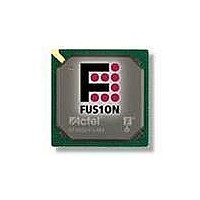
AFS250-FGG256 Actel, AFS250-FGG256 Datasheet - Page 24

AFS250-FGG256
Manufacturer Part Number
AFS250-FGG256
Description
FPGA - Field Programmable Gate Array 250K System Gates
Manufacturer
Actel
Datasheet
1.AFS600-PQG208.pdf
(330 pages)
Specifications of AFS250-FGG256
Processor Series
AFS250
Core
IP Core
Maximum Operating Frequency
1098.9 MHz
Number Of Programmable I/os
114
Data Ram Size
36864
Supply Voltage (max)
1.575 V
Maximum Operating Temperature
+ 70 C
Minimum Operating Temperature
0 C
Development Tools By Supplier
AFS-Eval-Kit, AFS-BRD600, FlashPro 3, FlashPro Lite, Silicon-Explorer II, Silicon-Sculptor 3, SI-EX-TCA
Mounting Style
SMD/SMT
Supply Voltage (min)
1.425 V
Number Of Gates
250 K
Package / Case
FPBGA-256
Lead Free Status / RoHS Status
Lead free / RoHS Compliant
Available stocks
Company
Part Number
Manufacturer
Quantity
Price
Company:
Part Number:
AFS250-FGG256
Manufacturer:
Actel
Quantity:
135
Company:
Part Number:
AFS250-FGG256
Manufacturer:
ACTEL
Quantity:
6 800
Company:
Part Number:
AFS250-FGG256I
Manufacturer:
Microsemi SoC
Quantity:
10 000
- Current page: 24 of 330
- Download datasheet (13Mb)
Device Architecture
Table 2-3 • Array Coordinates
Note:
Figure 2-7 • Array Coordinates for AFS600
2 - 8
Device
AFS090
AFS250
AFS600
AFS1500
VersaTile (Core)
VersaTile (Core)
Memory
Blocks
Memory
Blocks
The vertical I/O tile coordinates are not shown. West side coordinates are {(0, 2) to (2, 2)} to {(0, 77) to (2, 77)};
east side coordinates are {(195, 2) to (197, 2)} to {(195, 77) to (197, 77)}.
(0, 79)
(3, 75)
(3, 77)
(3, 76)
(0, 0)
(3, 4)
(3, 3)
(3, 2)
Array Coordinates
During many place-and-route operations in the Actel Designer software tool, it is possible to set
constraints that require array coordinates.
are measured from the lower left (0, 0). They can be used in region constraints for specific logic
groups/blocks, designated by a wildcard, and can contain core cells, memories, and I/Os.
Table 2-3
I/O and cell coordinates are used for placement constraints. Two coordinate systems are needed
because there is not a one-to-one correspondence between I/O cells and edge core cells. In addition, the
I/O coordinate system changes depending on the die/package combination. It is not listed in
The Designer ChipPlanner tool provides array coordinates of all I/O locations. I/O and cell coordinates
are used for placement constraints. However, I/O placement is easier by package pin assignment.
Figure 2-7
array coordinates for region/placement constraints, see the
(available in the software) for Fusion software tools.
Bottom Row (7, 0) to (165, 0)
x
3
3
3
3
Top Row (5, 1) to (168, 1)
I/O Tile to Analog Block
provides array coordinates of core cells and memory blocks.
Min.
illustrates the array coordinates of an AFS600 device. For more information on how to use
Bottom Row (5, 78) to (192, 78)
Top Row (7, 79) to (189, 79)
y
2
2
4
4
VersaTiles
I/O Tile
130
194
322
98
x
Max.
123
25
49
75
y
Table 2-3
R e vi s i o n 1
Bottom
(x, y)
None
None
(3, 2)
(3, 2)
is provided as a reference. The array coordinates
Memory Rows
Top Row (169, 1) to (192, 1)
UJTAG FlashROM
Designer User's Guide
(3, 124)
(3, 26)
(3, 50)
(3, 76)
(x, y)
Top
(x, y)
(0, 0)
(0, 0)
(0, 0)
(0, 0)
Min.
(197, 1)
(197, 0)
(194, 77)
(194, 76)
(194, 75)
VersaTile (Core)
(194, 4)
VersaTile(Core)
(194, 3)
(194, 2)
(197, 79)
All
or online help
(325, 129)
(101, 29)
(133, 53)
(197, 79)
Table
Memory
Blocks
(x, y)
Max.
Memory
Blocks
2-3.
Related parts for AFS250-FGG256
Image
Part Number
Description
Manufacturer
Datasheet
Request
R

Part Number:
Description:
FPGA 256/I�/Fusion Voltage: 1.5, 1.8, 2.5, 3.3 Mixed Voltage
Manufacturer:
Actel
Datasheet:

Part Number:
Description:
FPGA - Field Programmable Gate Array 250K System Gates
Manufacturer:
Actel
Datasheet:

Part Number:
Description:
MCU, MPU & DSP Development Tools Silicon Sculptor Programming Mod
Manufacturer:
Actel

Part Number:
Description:
MCU, MPU & DSP Development Tools InSystem Programming ProASICPLUS Devices
Manufacturer:
Actel

Part Number:
Description:
Programming Socket Adapters & Emulators PQ160 Module
Manufacturer:
Actel

Part Number:
Description:
Programming Socket Adapters & Emulators Axcelerator Adap Module Kit
Manufacturer:
Actel

Part Number:
Description:
Programming Socket Adapters & Emulators Evaluation
Manufacturer:
Actel

Part Number:
Description:
Programming Socket Adapters & Emulators AFDX Solutions
Manufacturer:
Actel

Part Number:
Description:
Programming Socket Adapters & Emulators SILICON SCULPTOR ADAPTER MODULE
Manufacturer:
Actel
Datasheet:

Part Number:
Description:
Programming Socket Adapters & Emulators Axcelerator Adap Module Kit
Manufacturer:
Actel

Part Number:
Description:
Programming Socket Adapters & Emulators Evaluation
Manufacturer:
Actel

Part Number:
Description:
Programming Socket Adapters & Emulators Silicon Sculptor Software
Manufacturer:
Actel

Part Number:
Description:
Programming Socket Adapters & Emulators InSystem Programming ProASICPLUS Devices
Manufacturer:
Actel


