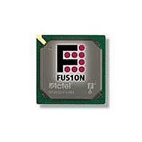
AFS250-FGG256 Actel, AFS250-FGG256 Datasheet - Page 328

AFS250-FGG256
Manufacturer Part Number
AFS250-FGG256
Description
FPGA - Field Programmable Gate Array 250K System Gates
Manufacturer
Actel
Datasheet
1.AFS600-PQG208.pdf
(330 pages)
Specifications of AFS250-FGG256
Processor Series
AFS250
Core
IP Core
Maximum Operating Frequency
1098.9 MHz
Number Of Programmable I/os
114
Data Ram Size
36864
Supply Voltage (max)
1.575 V
Maximum Operating Temperature
+ 70 C
Minimum Operating Temperature
0 C
Development Tools By Supplier
AFS-Eval-Kit, AFS-BRD600, FlashPro 3, FlashPro Lite, Silicon-Explorer II, Silicon-Sculptor 3, SI-EX-TCA
Mounting Style
SMD/SMT
Supply Voltage (min)
1.425 V
Number Of Gates
250 K
Package / Case
FPBGA-256
Lead Free Status / RoHS Status
Lead free / RoHS Compliant
Available stocks
Company
Part Number
Manufacturer
Quantity
Price
Company:
Part Number:
AFS250-FGG256
Manufacturer:
Actel
Quantity:
135
Company:
Part Number:
AFS250-FGG256
Manufacturer:
ACTEL
Quantity:
6 800
Company:
Part Number:
AFS250-FGG256I
Manufacturer:
Microsemi SoC
Quantity:
10 000
- Current page: 328 of 330
- Download datasheet (13Mb)
Datasheet Information
5- 12
Revision
Advance v0.3
(continued)
Figure 2-65 • Analog Block Macro
The
The
The
The
Information about the maximum pad input frequency was added to the
section.
The
EQ 2
The
Figure 2-16 • Fusion Clocking Options
Table 2-46 · Analog Channel Specifications
The notes in
Input Tolerance Capabilities
The
LVPECL and LVDS were updated in
Attributes vs. I/O Standard
LVPECL and LVDS were updated in
Standard
The
All voltage-referenced Minimum and Maximum DC Input and Output Level tables
were updated.
All Timing Characteristic tables were updated
Table 2-83 • Summary of Maximum and Minimum DC Input and Output Levels
Applicable to Commercial and Industrial Conditions
Table 2-79 • Summary of I/O Timing Characteristics – Software Default Settings
was updated.
Table 2-93 • I/O Output Buffer Maximum Resistances
The
standards included in the datasheet.
The
The
The
"Analog Quad" section
"Voltage Monitor" section
"Direct Digital Input" section
"Current Monitor" section
"Temperature Monitor" section
"ADC Description" section
"Simultaneously Switching Outputs and PCB Layout" section
"Timing Model"
"CoreMP7 and Cortex-M1 Software Tools" section
"108-Pin QFN" table
"180-Pin QFN" table
"208-Pin PQFP" table
"BLVDS/M-LVDS" section
"BLVDS/M-LVDS" section
is new.
Applications.
Table 2-72 • Fusion Standard and Advanced I/O – Hot-Swap and 5 V
was updated.
for the AFS090 device is new.
for the AFS090 device is new.
for the AFS090 device is new.
Applications.
was updated.
were updated.
was updated.
was updated.
was updated.
was updated.
is new. BLVDS and M-LVDS are two new I/O
is new. BLVDS and M-LVDS are two new I/O
was updated.
was updated.
Table 2-81 • Fusion Standard and Advanced I/O
R e visio n 1
Changes
Table 2-82 • Fusion Pro I/O Attributes vs. I/O
was updated.
was updated.
was updated.
was updated.
1
1
was updated.
is new.
was updated.
is new.
"Gate Driver"
2-103
2-102
2-144
2-149
2-157
2-158
2-161
2-165
2-134
2-171
2-257
2-165
2-134
2-171
Page
2-118
2-211
2-211
2-81
2-84
2-86
2-89
2-90
2-94
2-96
2-20
N/A
N/A
3-2
3-4
3-8
Related parts for AFS250-FGG256
Image
Part Number
Description
Manufacturer
Datasheet
Request
R

Part Number:
Description:
FPGA 256/I�/Fusion Voltage: 1.5, 1.8, 2.5, 3.3 Mixed Voltage
Manufacturer:
Actel
Datasheet:

Part Number:
Description:
FPGA - Field Programmable Gate Array 250K System Gates
Manufacturer:
Actel
Datasheet:

Part Number:
Description:
MCU, MPU & DSP Development Tools Silicon Sculptor Programming Mod
Manufacturer:
Actel

Part Number:
Description:
MCU, MPU & DSP Development Tools InSystem Programming ProASICPLUS Devices
Manufacturer:
Actel

Part Number:
Description:
Programming Socket Adapters & Emulators PQ160 Module
Manufacturer:
Actel

Part Number:
Description:
Programming Socket Adapters & Emulators Axcelerator Adap Module Kit
Manufacturer:
Actel

Part Number:
Description:
Programming Socket Adapters & Emulators Evaluation
Manufacturer:
Actel

Part Number:
Description:
Programming Socket Adapters & Emulators AFDX Solutions
Manufacturer:
Actel

Part Number:
Description:
Programming Socket Adapters & Emulators SILICON SCULPTOR ADAPTER MODULE
Manufacturer:
Actel
Datasheet:

Part Number:
Description:
Programming Socket Adapters & Emulators Axcelerator Adap Module Kit
Manufacturer:
Actel

Part Number:
Description:
Programming Socket Adapters & Emulators Evaluation
Manufacturer:
Actel

Part Number:
Description:
Programming Socket Adapters & Emulators Silicon Sculptor Software
Manufacturer:
Actel

Part Number:
Description:
Programming Socket Adapters & Emulators InSystem Programming ProASICPLUS Devices
Manufacturer:
Actel


