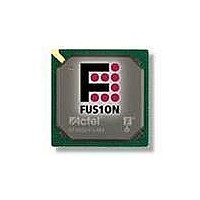
AFS250-FGG256 Actel, AFS250-FGG256 Datasheet - Page 74

AFS250-FGG256
Manufacturer Part Number
AFS250-FGG256
Description
FPGA - Field Programmable Gate Array 250K System Gates
Manufacturer
Actel
Datasheet
1.AFS600-PQG208.pdf
(330 pages)
Specifications of AFS250-FGG256
Processor Series
AFS250
Core
IP Core
Maximum Operating Frequency
1098.9 MHz
Number Of Programmable I/os
114
Data Ram Size
36864
Supply Voltage (max)
1.575 V
Maximum Operating Temperature
+ 70 C
Minimum Operating Temperature
0 C
Development Tools By Supplier
AFS-Eval-Kit, AFS-BRD600, FlashPro 3, FlashPro Lite, Silicon-Explorer II, Silicon-Sculptor 3, SI-EX-TCA
Mounting Style
SMD/SMT
Supply Voltage (min)
1.425 V
Number Of Gates
250 K
Package / Case
FPBGA-256
Lead Free Status / RoHS Status
Lead free / RoHS Compliant
Available stocks
Company
Part Number
Manufacturer
Quantity
Price
Company:
Part Number:
AFS250-FGG256
Manufacturer:
Actel
Quantity:
135
Company:
Part Number:
AFS250-FGG256
Manufacturer:
ACTEL
Quantity:
6 800
Company:
Part Number:
AFS250-FGG256I
Manufacturer:
Microsemi SoC
Quantity:
10 000
- Current page: 74 of 330
- Download datasheet (13Mb)
Device Architecture
2- 58
SRAM and FIFO
All Fusion devices have SRAM blocks along the north side of the device. Additionally, AFS600 and
AFS1500 devices have an SRAM block on the south side of the device. To meet the needs of high-
performance designs, the memory blocks operate strictly in synchronous mode for both read and write
operations. The read and write clocks are completely independent, and each may operate at any desired
frequency less than or equal to 350 MHz. The following configurations are available:
The Fusion SRAM memory block includes dedicated FIFO control logic to generate internal addresses
and external flag logic (FULL, EMPTY, AFULL, AEMPTY).
During RAM operation, addresses are sourced by the user logic, and the FIFO controller is ignored. In
FIFO mode, the internal addresses are generated by the FIFO controller and routed to the RAM array by
internal MUXes. Refer to
FIFO controller.
The Fusion architecture enables the read and write sizes of RAMs to be organized independently,
allowing for bus conversion. This is done with the WW (write width) and RW (read width) pins. The
different D×W configurations are 256×18, 512×9, 1k×4, 2k×2, and 4k×1. For example, the write size can
be set to 256×18 and the read size to 512×9.
Both the write and read widths for the RAM blocks can be specified independently with the WW (write
width) and RW (read width) pins. The different D×W configurations are 256×18, 512×9, 1k×4, 2k×2, and
4k×1.
Refer to the allowable RW and WW values supported for each of the RAM macro types in
page
When a width of one, two, or four is selected, the ninth bit is unused. For example, when writing 9-bit
values and reading 4-bit values, only the first four bits and the second four bits of each 9-bit value are
addressable for read operations. The ninth bit is not accessible.
•
•
•
2-61.
4k×1, 2k×2, 1k×4, 512×9 (dual-port RAM—two read, two write or one read, one write)
512×9, 256×18 (two-port RAM—one read and one write)
Sync write, sync pipelined/nonpipelined read
Figure 2-47
for more information about the implementation of the embedded
R e visio n 1
Table 2-27 on
Related parts for AFS250-FGG256
Image
Part Number
Description
Manufacturer
Datasheet
Request
R

Part Number:
Description:
FPGA 256/I�/Fusion Voltage: 1.5, 1.8, 2.5, 3.3 Mixed Voltage
Manufacturer:
Actel
Datasheet:

Part Number:
Description:
FPGA - Field Programmable Gate Array 250K System Gates
Manufacturer:
Actel
Datasheet:

Part Number:
Description:
MCU, MPU & DSP Development Tools Silicon Sculptor Programming Mod
Manufacturer:
Actel

Part Number:
Description:
MCU, MPU & DSP Development Tools InSystem Programming ProASICPLUS Devices
Manufacturer:
Actel

Part Number:
Description:
Programming Socket Adapters & Emulators PQ160 Module
Manufacturer:
Actel

Part Number:
Description:
Programming Socket Adapters & Emulators Axcelerator Adap Module Kit
Manufacturer:
Actel

Part Number:
Description:
Programming Socket Adapters & Emulators Evaluation
Manufacturer:
Actel

Part Number:
Description:
Programming Socket Adapters & Emulators AFDX Solutions
Manufacturer:
Actel

Part Number:
Description:
Programming Socket Adapters & Emulators SILICON SCULPTOR ADAPTER MODULE
Manufacturer:
Actel
Datasheet:

Part Number:
Description:
Programming Socket Adapters & Emulators Axcelerator Adap Module Kit
Manufacturer:
Actel

Part Number:
Description:
Programming Socket Adapters & Emulators Evaluation
Manufacturer:
Actel

Part Number:
Description:
Programming Socket Adapters & Emulators Silicon Sculptor Software
Manufacturer:
Actel

Part Number:
Description:
Programming Socket Adapters & Emulators InSystem Programming ProASICPLUS Devices
Manufacturer:
Actel


