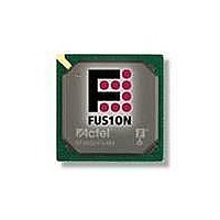
AFS250-FGG256 Actel, AFS250-FGG256 Datasheet - Page 326

AFS250-FGG256
Manufacturer Part Number
AFS250-FGG256
Description
FPGA - Field Programmable Gate Array 250K System Gates
Manufacturer
Actel
Datasheet
1.AFS600-PQG208.pdf
(330 pages)
Specifications of AFS250-FGG256
Processor Series
AFS250
Core
IP Core
Maximum Operating Frequency
1098.9 MHz
Number Of Programmable I/os
114
Data Ram Size
36864
Supply Voltage (max)
1.575 V
Maximum Operating Temperature
+ 70 C
Minimum Operating Temperature
0 C
Development Tools By Supplier
AFS-Eval-Kit, AFS-BRD600, FlashPro 3, FlashPro Lite, Silicon-Explorer II, Silicon-Sculptor 3, SI-EX-TCA
Mounting Style
SMD/SMT
Supply Voltage (min)
1.425 V
Number Of Gates
250 K
Package / Case
FPBGA-256
Lead Free Status / RoHS Status
Lead free / RoHS Compliant
Available stocks
Company
Part Number
Manufacturer
Quantity
Price
Company:
Part Number:
AFS250-FGG256
Manufacturer:
Actel
Quantity:
135
Company:
Part Number:
AFS250-FGG256
Manufacturer:
ACTEL
Quantity:
6 800
Company:
Part Number:
AFS250-FGG256I
Manufacturer:
Microsemi SoC
Quantity:
10 000
- Current page: 326 of 330
- Download datasheet (13Mb)
Datasheet Information
5- 10
Revision
Advance v0.6
(October 2006)
The second paragraph of the
information about POWERDOWN.
The description for bit 0 was updated in
3.9 was changed to 7.8 in the
All function descriptions in
In
updated.
The
The
Table 2-35 • FIFO
The VAREF function description was updated in
Description.
The
mode and sleep mode.
The text in the
The
the drain.
The
statement:
"All results are MSB justified in the ADC."
The information about the ADCSTART signal was updated in the
section.
Table 2-46 · Analog Channel Specifications
Table 2-47 · ADC Characteristics in Direct Input Mode
Table 2-51 • ACM Address Decode Table for Analog Quad
In
Setting for Bit 6 in Byte 3 was updated.
The
outputs, and bibufs.
In
updated for the following features:
Single-ended receiver
Voltage-referenced differential receiver
LVDS/LVPECL differential receiver features
The
descriptions
The
information about avoiding high current draw.
The
include information about avoiding high current draw.
The
statement: VMV and V
pins within a given I/O bank.
Table 2-69 • Fusion Pro I/O
Table 2-19 • Flash Memory Block Pin
Table 2-53 • Analog Quad ACM Byte
"RESET" section
"RESET" section
"Voltage Monitor" section
"Gate Driver" section
"Introduction" section
"V
"User I/O Naming Convention" section
"Analog-to-Digital Converter Block" section
"V
"VMVx I/O Supply Voltage (quiet)" section
CCNVM
CC33PMP
Flash Memory Block Power Supply (1.5 V)" section
"Current Monitor" section
Analog Power Supply (3.3 V)" section
was updated.
was updated.
was updated.
CCI
Table 2-18 · Signals for VRPSM
was updated to include information about forcing 1 V on
must be connected to the same power supply and V
was updated to include information about digital inputs,
"Crystal Oscillator (Xtal Osc)"
was updated to include information about low power
Features, the programmable delay descriptions were
"PLL Macro" section
R e visio n 1
Changes
Table 2-17 · RTC Control/Status
was changed from 2 mV to 1 mV.
was updated.
Assignment, the Function and Default
Names, the RD[31:0] description was
was updated to include "V" and "z"
was updated with the following
Table 2-36 • Analog Block Pin
was updated to include this
was updated.
was updated to include
was updated to include
Macro.
section.
was updated.
"ADC Description"
was updated to
Register.
CCI
2-102
2-121
2-127
2-130
2-133
2-137
2-159
2-224
2-224
2-185
Page
2-118
2-40.
2-30
2-38
2-42
2-43
2-61
2-64
2-79
2-82
2-86
2-90
2-94
2-99
Related parts for AFS250-FGG256
Image
Part Number
Description
Manufacturer
Datasheet
Request
R

Part Number:
Description:
FPGA 256/I�/Fusion Voltage: 1.5, 1.8, 2.5, 3.3 Mixed Voltage
Manufacturer:
Actel
Datasheet:

Part Number:
Description:
FPGA - Field Programmable Gate Array 250K System Gates
Manufacturer:
Actel
Datasheet:

Part Number:
Description:
MCU, MPU & DSP Development Tools Silicon Sculptor Programming Mod
Manufacturer:
Actel

Part Number:
Description:
MCU, MPU & DSP Development Tools InSystem Programming ProASICPLUS Devices
Manufacturer:
Actel

Part Number:
Description:
Programming Socket Adapters & Emulators PQ160 Module
Manufacturer:
Actel

Part Number:
Description:
Programming Socket Adapters & Emulators Axcelerator Adap Module Kit
Manufacturer:
Actel

Part Number:
Description:
Programming Socket Adapters & Emulators Evaluation
Manufacturer:
Actel

Part Number:
Description:
Programming Socket Adapters & Emulators AFDX Solutions
Manufacturer:
Actel

Part Number:
Description:
Programming Socket Adapters & Emulators SILICON SCULPTOR ADAPTER MODULE
Manufacturer:
Actel
Datasheet:

Part Number:
Description:
Programming Socket Adapters & Emulators Axcelerator Adap Module Kit
Manufacturer:
Actel

Part Number:
Description:
Programming Socket Adapters & Emulators Evaluation
Manufacturer:
Actel

Part Number:
Description:
Programming Socket Adapters & Emulators Silicon Sculptor Software
Manufacturer:
Actel

Part Number:
Description:
Programming Socket Adapters & Emulators InSystem Programming ProASICPLUS Devices
Manufacturer:
Actel


