OM13005,598 NXP Semiconductors, OM13005,598 Datasheet - Page 45
OM13005,598
Manufacturer Part Number
OM13005,598
Description
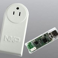
BOARD EVAL EM773 METER US PLUG
Manufacturer
NXP Semiconductors
Type
Other Power Managementr
Specifications of OM13005,598
Design Resources
Plug Meter Schematics, Gerber Files USB Dongle Schematics, Gerber Files
Main Purpose
Power Management, Energy/Power Meter
Embedded
Yes, MCU, 32-Bit
Utilized Ic / Part
EM773FHN33,551
Interface Type
USB
Maximum Operating Temperature
+ 150 C
Operating Supply Voltage
1.8 V to 3.6 V
Product
Power Management Development Tools
Lead Free Status / RoHS Status
Lead free / RoHS Compliant
Primary Attributes
-
Secondary Attributes
-
Lead Free Status / Rohs Status
Lead free / RoHS Compliant
For Use With/related Products
EM773, OL2381
Other names
568-6680


NXP Semiconductors
Table 47.
UM10415
User manual
Name
-
IOCON_PIO2_0
IOCON_RESET_PIO0_0
IOCON_PIO0_1
IOCON_PIO1_8
-
IOCON_PIO0_2
IOCON_PIO0_3
IOCON_PIO0_4
IOCON_PIO0_5
IOCON_PIO1_9
IOCON_PIO3_4
IOCON_PIO3_5
IOCON_PIO0_6
IOCON_PIO0_7
IOCON_PIO0_8
IOCON_PIO0_9
IOCON_SWCLK_PIO0_10
IOCON_R_PIO1_1
IOCON_R_PIO1_2
IOCON_SWDIO_PIO1_3
IOCON_PIO1_4
IOCON_PIO1_11
IOCON_PIO3_2
IOCON_PIO1_5
Register overview: I/O configuration (base address 0x4004 4000)
Each port pin PIOn_m has one IOCON register assigned to control the pin’s function and
electrical characteristics.
Some input functions (SCK0, DSR0, DCD0, and RI0) are multiplexed to several physical
pins. The IOCON_LOC registers select the pin location for each of these functions.
Remark: The IOCON registers are listed in order of their memory locations in
Access
R/W
R/W
R/W
R/W
R/W
R/W
R/W
R/W
R/W
R/W
R/W
R/W
R/W
R/W
R/W
R/W
R/W
R/W
R/W
R/W
R/W
R/W
R/W
R/W
R/W
All information provided in this document is subject to legal disclaimers.
Address
offset
0x004
0x008
0x00C
0x010
0x014
0x018
0x01C
0x02C
0x030
0x034
0x038
0x03C
0x048
0x04C
0x050
0x060
0x064
0x068
0x07C
0x080
0x090
0x094
0x098
0x09C
0x0A0
Rev. 1 — 10 September 2010
Description
Reserved
I/O configuration for pin
PIO2_0/DTR/SSEL1
I/O configuration for pin RESET/PIO0_0 0xD0
I/O configuration for pin
PIO0_1/CLKOUT/CT32B0_MAT2
I/O configuration for pin PIO1_8
Reserved
I/O configuration for pin
PIO0_2/SSEL0/CT16B0_CAP0
I/O configuration for pin PIO0_3
I/O configuration for pin PIO0_4/SCL
I/O configuration for pin PIO0_5/SDA
I/O configuration for pin PIO1_9
I/O configuration for pin PIO3_4
I/O configuration for pin PIO3_5
I/O configuration for pin PIO0_6/SCK0
I/O configuration for pin PIO0_7/CTS
I/O configuration for pin
PIO0_8/MISO0/CT16B0_MAT0
I/O configuration for pin
PIO0_9/MOSI0/CT16B0_MAT1
I/O configuration for pin
SWCLK/PIO0_10/
SCK0/CT16B0_MAT2
I/O configuration for pin
R/PIO1_1/CT32B1_MAT0
I/O configuration for pin
R/PIO1_2/CT32B1_MAT1
I/O configuration for pin
SWDIO/PIO1_3/CT32B1_MAT2
I/O configuration for pin
PIO1_4/CT32B1_MAT3
I/O configuration for pin PIO1_11
I/O configuration for pin PIO3_2/DCD
I/O configuration for pin
PIO1_5/RTS/CT32B0_CAP0
Chapter 6: EM773 I/O Configuration
Reset
value
-
0xD0
0xD0
0xD0
-
0xD0
0xD0
0x00
0x00
0xD0
0xD0
0xD0
0xD0
0xD0
0xD0
0xD0
0xD0
0xD0
0xD0
0xD0
0xD0
0xD0
0xD0
0xD0
UM10415
© NXP B.V. 2010. All rights reserved.
Reference
-
Table 49
Table 50
Table 51
Table 52
-
Table 53
Table 54
Table 55
Table 56
Table 57
Table 58
Table 59
Table 60
Table 61
Table 62
Table 63
Table 64
Table 65
Table 66
Table 67
Table 68
Table 69
Table 70
Table 71
Table
45 of 310
47.
Related parts for OM13005,598
Image
Part Number
Description
Manufacturer
Datasheet
Request
R

Part Number:
Description:
NXP Semiconductors designed the LPC2420/2460 microcontroller around a 16-bit/32-bitARM7TDMI-S CPU core with real-time debug interfaces that include both JTAG andembedded trace
Manufacturer:
NXP Semiconductors
Datasheet:

Part Number:
Description:
NXP Semiconductors designed the LPC2458 microcontroller around a 16-bit/32-bitARM7TDMI-S CPU core with real-time debug interfaces that include both JTAG andembedded trace
Manufacturer:
NXP Semiconductors
Datasheet:
Part Number:
Description:
NXP Semiconductors designed the LPC2468 microcontroller around a 16-bit/32-bitARM7TDMI-S CPU core with real-time debug interfaces that include both JTAG andembedded trace
Manufacturer:
NXP Semiconductors
Datasheet:
Part Number:
Description:
NXP Semiconductors designed the LPC2470 microcontroller, powered by theARM7TDMI-S core, to be a highly integrated microcontroller for a wide range ofapplications that require advanced communications and high quality graphic displays
Manufacturer:
NXP Semiconductors
Datasheet:
Part Number:
Description:
NXP Semiconductors designed the LPC2478 microcontroller, powered by theARM7TDMI-S core, to be a highly integrated microcontroller for a wide range ofapplications that require advanced communications and high quality graphic displays
Manufacturer:
NXP Semiconductors
Datasheet:
Part Number:
Description:
The Philips Semiconductors XA (eXtended Architecture) family of 16-bit single-chip microcontrollers is powerful enough to easily handle the requirements of high performance embedded applications, yet inexpensive enough to compete in the market for hi
Manufacturer:
NXP Semiconductors
Datasheet:
Part Number:
Description:
The XA-S3 device is a member of Philips Semiconductors? XA(eXtended Architecture) family of high performance 16-bitsingle-chip microcontrollers
Manufacturer:
NXP Semiconductors
Datasheet:

Part Number:
Description:
The NXP BlueStreak LH75401/LH75411 family consists of two low-cost 16/32-bit System-on-Chip (SoC) devices
Manufacturer:
NXP Semiconductors
Datasheet:
Part Number:
Description:
The NXP LPC3130/3131 combine an 180 MHz ARM926EJ-S CPU core, high-speed USB2
Manufacturer:
NXP Semiconductors
Datasheet:
Part Number:
Description:
The NXP LPC3141 combine a 270 MHz ARM926EJ-S CPU core, High-speed USB 2
Manufacturer:
NXP Semiconductors
Part Number:
Description:
The NXP LPC3143 combine a 270 MHz ARM926EJ-S CPU core, High-speed USB 2
Manufacturer:
NXP Semiconductors

Part Number:
Description:
The NXP LPC3152 combines an 180 MHz ARM926EJ-S CPU core, High-speed USB 2
Manufacturer:
NXP Semiconductors
Part Number:
Description:
The NXP LPC3154 combines an 180 MHz ARM926EJ-S CPU core, High-speed USB 2
Manufacturer:
NXP Semiconductors

Part Number:
Description:
Standard level N-channel enhancement mode Field-Effect Transistor (FET) in a plastic package using NXP High-Performance Automotive (HPA) TrenchMOS technology
Manufacturer:
NXP Semiconductors
Datasheet: