OM13006,598 NXP Semiconductors, OM13006,598 Datasheet - Page 107
OM13006,598
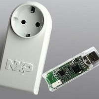
Manufacturer Part Number
OM13006,598
Description
BOARD EVAL EM773 METER EU PLUG
Manufacturer
NXP Semiconductors
Type
Other Power Managementr
Specifications of OM13006,598
Design Resources
Plug Meter Schematics, Gerber Files USB Dongle Schematics, Gerber Files
Main Purpose
Power Management, Energy/Power Meter
Embedded
Yes, MCU, 32-Bit
Utilized Ic / Part
EM773FHN33,551
Interface Type
USB
Maximum Operating Temperature
+ 150 C
Operating Supply Voltage
1.8 V to 3.6 V
Product
Power Management Development Tools
Lead Free Status / RoHS Status
Lead free / RoHS Compliant
Primary Attributes
-
Secondary Attributes
-
Lead Free Status / Rohs Status
Lead free / RoHS Compliant
For Use With/related Products
EM773, OL2381
Other names
568-6681


NXP Semiconductors
10.9 I
UM10415
User manual
2
C operating modes
10.8.10 I
10.9.1 Master Transmitter mode
Table 123. I
The four mask registers each contain seven active bits (7:1). Any bit in these registers
which is set to ‘1’ will cause an automatic compare on the corresponding bit of the
received address when it is compared to the I2ADDRn register associated with that mask
register. In other words, bits in an I2ADDRn register which are masked are not taken into
account in determining an address match.
On reset, all mask register bits are cleared to ‘0’.
The mask register has no effect on comparison to the General Call address (“0000000”).
Bits(31:8) and bit(0) of the mask registers are unused and should not be written to. These
bits will always read back as zeros.
When an address-match interrupt occurs, the processor will have to read the data register
(I2DAT) to determine what the received address was that actually caused the match.
Table 124. I
In a given application, the I
mode, the I
address. If one of these addresses is detected, an interrupt is requested. If the processor
wishes to become the bus master, the hardware waits until the bus is free before the
master mode is entered so that a possible slave operation is not interrupted. If bus
arbitration is lost in the master mode, the I
immediately and can detect its own slave address in the same serial transfer.
In this mode data is transmitted from master to slave. Before the master transmitter mode
can be entered, the I2CONSET register must be initialized as shown in
must be set to 1 to enable the I
acknowledge any address when another device is master of the bus, so it can not enter
slave mode. The STA, STO and SI bits must be 0. The SI Bit is cleared by writing 1 to the
SIC bit in the I2CONCLR register. THe STA bit should be cleared after writing the slave
address.
Bit
7:0
31:8 -
Bit
0
7:1
31:8
2
C Mask registers (I2C0MASK[0, 1, 2, 3] - 0x4000 00[30, 34, 38, 3C])
Symbol
Data
Symbol
-
MASK
-
description
2
2
2
C hardware looks for any one of its four slave addresses and the General Call
C Data buffer register (I2C0DATA_BUFFER - 0x4000 002C) bit description
C Mask registers (I2C0MASK[0, 1, 2, 3] - 0x4000 00[30, 34, 38, 3C]) bit
All information provided in this document is subject to legal disclaimers.
Description
This register holds contents of the 8 MSBs of the I2DAT shift
register.
Reserved. The value read from a reserved bit is not defined.
Description
Reserved. User software should not write ones to reserved
bits. This bit reads always back as 0.
Mask bits.
Reserved. The value read from reserved bits is undefined.
Rev. 1 — 10 September 2010
2
C block may operate as a master, a slave, or both. In the slave
2
C function. If the AA bit is 0, the I
2
C block switches to the slave mode
Chapter 10: EM773 I2C-bus interface
2
C interface will not
UM10415
© NXP B.V. 2010. All rights reserved.
Table
Reset value
0
0x00
0
Reset value
0
0
125. I2EN
107 of 310
Related parts for OM13006,598
Image
Part Number
Description
Manufacturer
Datasheet
Request
R

Part Number:
Description:
NXP Semiconductors designed the LPC2420/2460 microcontroller around a 16-bit/32-bitARM7TDMI-S CPU core with real-time debug interfaces that include both JTAG andembedded trace
Manufacturer:
NXP Semiconductors
Datasheet:

Part Number:
Description:
NXP Semiconductors designed the LPC2458 microcontroller around a 16-bit/32-bitARM7TDMI-S CPU core with real-time debug interfaces that include both JTAG andembedded trace
Manufacturer:
NXP Semiconductors
Datasheet:
Part Number:
Description:
NXP Semiconductors designed the LPC2468 microcontroller around a 16-bit/32-bitARM7TDMI-S CPU core with real-time debug interfaces that include both JTAG andembedded trace
Manufacturer:
NXP Semiconductors
Datasheet:
Part Number:
Description:
NXP Semiconductors designed the LPC2470 microcontroller, powered by theARM7TDMI-S core, to be a highly integrated microcontroller for a wide range ofapplications that require advanced communications and high quality graphic displays
Manufacturer:
NXP Semiconductors
Datasheet:
Part Number:
Description:
NXP Semiconductors designed the LPC2478 microcontroller, powered by theARM7TDMI-S core, to be a highly integrated microcontroller for a wide range ofapplications that require advanced communications and high quality graphic displays
Manufacturer:
NXP Semiconductors
Datasheet:
Part Number:
Description:
The Philips Semiconductors XA (eXtended Architecture) family of 16-bit single-chip microcontrollers is powerful enough to easily handle the requirements of high performance embedded applications, yet inexpensive enough to compete in the market for hi
Manufacturer:
NXP Semiconductors
Datasheet:
Part Number:
Description:
The XA-S3 device is a member of Philips Semiconductors? XA(eXtended Architecture) family of high performance 16-bitsingle-chip microcontrollers
Manufacturer:
NXP Semiconductors
Datasheet:

Part Number:
Description:
The NXP BlueStreak LH75401/LH75411 family consists of two low-cost 16/32-bit System-on-Chip (SoC) devices
Manufacturer:
NXP Semiconductors
Datasheet:
Part Number:
Description:
The NXP LPC3130/3131 combine an 180 MHz ARM926EJ-S CPU core, high-speed USB2
Manufacturer:
NXP Semiconductors
Datasheet:
Part Number:
Description:
The NXP LPC3141 combine a 270 MHz ARM926EJ-S CPU core, High-speed USB 2
Manufacturer:
NXP Semiconductors
Part Number:
Description:
The NXP LPC3143 combine a 270 MHz ARM926EJ-S CPU core, High-speed USB 2
Manufacturer:
NXP Semiconductors

Part Number:
Description:
The NXP LPC3152 combines an 180 MHz ARM926EJ-S CPU core, High-speed USB 2
Manufacturer:
NXP Semiconductors
Part Number:
Description:
The NXP LPC3154 combines an 180 MHz ARM926EJ-S CPU core, High-speed USB 2
Manufacturer:
NXP Semiconductors

Part Number:
Description:
Standard level N-channel enhancement mode Field-Effect Transistor (FET) in a plastic package using NXP High-Performance Automotive (HPA) TrenchMOS technology
Manufacturer:
NXP Semiconductors
Datasheet: