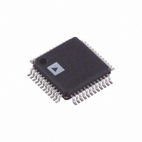
ADUC7032BSTZ-8L-RL Analog Devices Inc, ADUC7032BSTZ-8L-RL Datasheet - Page 105

ADUC7032BSTZ-8L-RL
Manufacturer Part Number
ADUC7032BSTZ-8L-RL
Description
IC,Battery Management,QFP,48PIN,PLASTIC
Manufacturer
Analog Devices Inc
Series
MicroConverter® ADuC7xxxr
Datasheet
1.EVAL-ADUC7032QSPZ.pdf
(116 pages)
Specifications of ADUC7032BSTZ-8L-RL
Core Processor
ARM7
Core Size
16/32-Bit
Speed
20.48MHz
Connectivity
LIN, SPI, UART/USART
Peripherals
POR, PSM, Temp Sensor, WDT
Number Of I /o
9
Program Memory Size
96KB (96K x 8)
Program Memory Type
FLASH
Ram Size
6K x 8
Voltage - Supply (vcc/vdd)
3.5 V ~ 18 V
Data Converters
A/D 2x16b
Oscillator Type
Internal
Operating Temperature
-40°C ~ 105°C
Package / Case
48-LQFP
Lead Free Status / RoHS Status
Lead free / RoHS Compliant
Eeprom Size
-
Lead Free Status / Rohs Status
Compliant
LIN Hardware Synchronization Control Register 1
Name: LHSCON1
Address: 0xFFFF078C
Default Value: 0x32
Access: Read/write
Function: This LHS control register is an 8-bit register that, in conjunction with the LHSCON0 register, is used to configure the LIN
mode of operation.
Table 93. LHSCON1 MMR Bit Designations
Bit
7 to 4
3 to 0
LIN Hardware Synchronization Timer0 Register
Name: LHSVAL0
Address: 0xFFFF0788
Default Value: 0x0000
Access: Read/write
Function: This 16-bit read-only register holds the value of the
internal LIN synchronization timer. The LIN synchronization
timer is clocked from an internal 5 MHz clock that is independent
of core clock and baud rate frequency. In LIN mode, the value
read by user code from the LHSVAL0 register can be used to
calculate the master LIN baud rate. This calculation can then be
used to configure the internal UART baud rate to ensure correct
LIN communication via the UART from the ADuC7032-8L
slave to the LIN master node.
LIN Hardware Break Timer1 Register
Name: LHSVAL1
Address: 0xFFFF0790
Default Value: 0x000 (read) or 0x047 (write)
Access: Read/write
Function: When user code reads this location, the 12-bit value
returned is the value of the internal LIN break timer, which is
clocked directly from the on-chip low power (131 kHz)
oscillator and times the LIN break pulse.
Description
LIN Stop Edge Count. These four bits are set by user code to the number of falling or rising edges on which to stop the internal LIN
synchronization counter. The stop value of this counter can be read by user code via LHSVAL0. The type of edge, either rising or
falling, is configured by LHSCON0[7]. The default value of these bits is 0x3, which configures the hardware to stop counting on the
third falling edge. It should be noted that the first falling edge is taken as the falling edge at the start of the LIN break pulse.
LIN Start Edge Count. These four bits are set by user code to the number of falling edges after which the internal LIN
synchronization timer starts counting. The stop value of this counter can be read by user code via LHSVAL0. The default value of
these bits is 0x2, which configures the hardware to start counting on the second falling edge. It should be noted that the first
falling edge is taken as the falling edge at the start of the LIN break pulse.
Rev.0 | Page 105 of 116
A negative edge on the LIN bus or user code reading the LHSVAL1
results in the timer and the register contents being reset to 0. When
user code writes to this location, the 12-bit value is actually written
not to the LIN break timer, but to a LIN break compare register.
In LIN mode of operation, the value in the compare register is
continuously compared to the break timer value. A LIN break
interrupt (IRQEN[7] and LHSSTA[0]) is generated when the
timer value reaches the compare value. After the break condition
interrupt, the LIN break timer continues to count until the rising
edge of the break signal. If a rising edge is not detected and the
12-bit timer overflows (4096 × 1/131 kHz = 31 ms), a break field
error interrupt (IRQEN[7] and LHSSTA[4]) is generated. By
default, the value in the compare register is 0x47, corresponding
to 11-bit periods, that is, the minimum pulse width for a LIN
break pulse at 20 kbps. For different baud rates, this value can
be changed by writing to LHSVAL1. It is also important to note
that if a valid break interrupt is not received, subsequent sync
pulse timing through the LHSVAL0 register does not occur.
ADuC7032-8L


