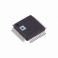
ADUC7032BSTZ-8L-RL Analog Devices Inc, ADUC7032BSTZ-8L-RL Datasheet - Page 15

ADUC7032BSTZ-8L-RL
Manufacturer Part Number
ADUC7032BSTZ-8L-RL
Description
IC,Battery Management,QFP,48PIN,PLASTIC
Manufacturer
Analog Devices Inc
Series
MicroConverter® ADuC7xxxr
Datasheet
1.EVAL-ADUC7032QSPZ.pdf
(116 pages)
Specifications of ADUC7032BSTZ-8L-RL
Core Processor
ARM7
Core Size
16/32-Bit
Speed
20.48MHz
Connectivity
LIN, SPI, UART/USART
Peripherals
POR, PSM, Temp Sensor, WDT
Number Of I /o
9
Program Memory Size
96KB (96K x 8)
Program Memory Type
FLASH
Ram Size
6K x 8
Voltage - Supply (vcc/vdd)
3.5 V ~ 18 V
Data Converters
A/D 2x16b
Oscillator Type
Internal
Operating Temperature
-40°C ~ 105°C
Package / Case
48-LQFP
Lead Free Status / RoHS Status
Lead free / RoHS Compliant
Eeprom Size
-
Lead Free Status / Rohs Status
Compliant
PIN CONFIGURATION AND FUNCTION DESCRIPTIONS
Table 7. Pin Function Descriptions
Pin No.
1
2
3
4
5
Mnemonic
RESET
GPIO_5/IRQ1/RxD
GPIO_6/TxD
GPIO_7/IRQ4
GPIO_8/IRQ5
GPIO_5/IRQ1/RxD
GPIO_7/IRQ4
GPIO_8/IRQ5
Type
I
I/O
I/O
I/O
I/O
GPIO_6/TxD
RESET
NTRST
1
DGND
TDO
TMS
TCK
TDI
NC
NC = NO CONNECT
Description
Reset Input Pin, Active Low. This pin has an internal, weak, pull-up resistor to REG_DVDD. When
not in use, this pin remains unconnected. For added security and robustness, it is recommended
that this pin be strapped, via a resistor, to REG_DVDD.
General-Purpose Digital Input/Output 5, External Interrupt Request 1, or Receive Data. By default
and after power-on reset, this pin is configured as an input. The pin has an internal, weak, pull-up
resistor and, when not in use, it can be left unconnected. This multifunction pin can be configured
in one of three states, namely
This pin can also be used as a clock input to Timer1.
General-Purpose Digital Input/Output 6 or Transmit Data. By default and after power-on reset, this
pin is configured as an input. The pin has an internal, weak, pull-up resistor and, when not in use,
it can be left unconnected. This multifunction pin can be configured in one of two states, namely
General-Purpose Digital Input/Output 7 or External Interrupt Request 4. By default and after
power-on reset, this pin is configured as an input. The pin has an internal, weak, pull-up resistor and,
when not in use, it can be left unconnected. This multifunction pin can be configured in one of
two states, namely
General-Purpose Digital Input/Output 8 or External Interrupt Request 5. By default and after
power-on reset, this pin is configured as an input. The pin has an internal, weak, pull-up resistor
and, when not in use, it can be left unconnected. This multifunction pin can be configured in
one of two states, namely
This pin can also be used as a clock input to Timer1.
10
11
12
General-Purpose Digital I/O 5.
External Interrupt Request 1, active high.
Receive data for UART serial port.
General-Purpose Digital I/O 6.
Transmit data for UART serial port.
General-Purpose Digital I/O 7.
External Interrupt Request 4, active high.
General-Purpose Digital I/O 8.
External Interrupt Request 5, active high.
1
2
3
4
5
6
7
8
9
IDENTIFIER
PIN 1
Figure 8. Pin Configuration
Rev.0 | Page 15 of 116
ADuC7032-8L
(Not to Scale)
TOP VIEW
36
35
34
33
32
31
30
29
28
27
26
25
XTAL1
DGND
DGND
REG_DVDD
NC
GPIO_4/ECLK
GPIO_3/MOSI
GPIO_2/MISO
GPIO_1/SCLK
GPIO_0/IRQ0/SS
NC
NC
ADuC7032-8L


