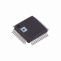
ADUC7032BSTZ-8L-RL Analog Devices Inc, ADUC7032BSTZ-8L-RL Datasheet - Page 62

ADUC7032BSTZ-8L-RL
Manufacturer Part Number
ADUC7032BSTZ-8L-RL
Description
IC,Battery Management,QFP,48PIN,PLASTIC
Manufacturer
Analog Devices Inc
Series
MicroConverter® ADuC7xxxr
Datasheet
1.EVAL-ADUC7032QSPZ.pdf
(116 pages)
Specifications of ADUC7032BSTZ-8L-RL
Core Processor
ARM7
Core Size
16/32-Bit
Speed
20.48MHz
Connectivity
LIN, SPI, UART/USART
Peripherals
POR, PSM, Temp Sensor, WDT
Number Of I /o
9
Program Memory Size
96KB (96K x 8)
Program Memory Type
FLASH
Ram Size
6K x 8
Voltage - Supply (vcc/vdd)
3.5 V ~ 18 V
Data Converters
A/D 2x16b
Oscillator Type
Internal
Operating Temperature
-40°C ~ 105°C
Package / Case
48-LQFP
Lead Free Status / RoHS Status
Lead free / RoHS Compliant
Eeprom Size
-
Lead Free Status / Rohs Status
Compliant
- Current page: 62 of 116
- Download datasheet (3Mb)
ADuC7032-8L
PLLCON Prewrite Key PLLKEY0
Name: PLLKEY0
Address: 0xFFFF0410
Access: Write only
Key: 0x000000AA
Function: PLLCON is a keyed register that requires a 32-bit key
value to be written before and after PLLCON. PLLKEY0 is the
prewrite key.
PLLCON Postwrite Key PLLKEY1
Name: PLLKEY1
Address: 0xFFFF0418
Access: Write only
Key: 0x00000055
Function: PLLCON is a keyed register that requires a 32-bit key
value to be written before and after PLLCON. PLLKEY1 is the
postwrite key.
Rev.0 | Page 62 of 116
1
PLLCON Register
Name: PLLCON
Address: 0xFFFF0414
Default Value: 0x00
Access: Read/write
Function: This 8-bit register allows user code to dynamically
select the PLL source clock from three different oscillator sources.
Table 46. PLLCON MMR Bit Designations
Bit
31 to 3
2
1 to 0
If user code switches MCU clock sources, a dummy MCU cycle should be
included after the clock switch is written to PLLCON.
Description
Reserved. These bits should be written as 0 by user code.
Not Used. Must be written as 0 by user software.
PLL Clock Source.
00 = low power 131 kHz oscillator.
01 = precision 131 kHz oscillator.
10 = external 32.768 kHz crystal.
11 = reserved.
1
Related parts for ADUC7032BSTZ-8L-RL
Image
Part Number
Description
Manufacturer
Datasheet
Request
R

Part Number:
Description:
Integrated Precision Battery Sensor For Automotive System
Manufacturer:
Analog Devices, Inc.
Datasheet:

Part Number:
Description:
Microconverter Integrated, Precision Battery Sensor
Manufacturer:
Analog Devices, Inc.
Datasheet:

Part Number:
Description:
±1.7g Dual-Axis IMEMS Accelerometer Evaluation Board
Manufacturer:
Analog Devices Inc
Datasheet:

Part Number:
Description:
Inertial Sensor Evaluation System
Manufacturer:
Analog Devices Inc
Datasheet:

Part Number:
Description:
Manufacturer:
Analog Devices Inc
Datasheet:

Part Number:
Description:
Manufacturer:
Analog Devices Inc
Datasheet:

Part Number:
Description:
Manufacturer:
Analog Devices Inc
Datasheet:

Part Number:
Description:
Manufacturer:
Analog Devices Inc
Datasheet:

Part Number:
Description:
Manufacturer:
Analog Devices Inc
Datasheet:

Part Number:
Description:
Manufacturer:
Analog Devices Inc
Datasheet:

Part Number:
Description:
Manufacturer:
Analog Devices Inc
Datasheet:

Part Number:
Description:
Manufacturer:
Analog Devices Inc
Datasheet:

Part Number:
Description:
Manufacturer:
Analog Devices Inc
Datasheet:


