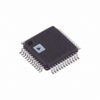
ADUC7032BSTZ-8L-RL Analog Devices Inc, ADUC7032BSTZ-8L-RL Datasheet - Page 21

ADUC7032BSTZ-8L-RL
Manufacturer Part Number
ADUC7032BSTZ-8L-RL
Description
IC,Battery Management,QFP,48PIN,PLASTIC
Manufacturer
Analog Devices Inc
Series
MicroConverter® ADuC7xxxr
Datasheet
1.EVAL-ADUC7032QSPZ.pdf
(116 pages)
Specifications of ADUC7032BSTZ-8L-RL
Core Processor
ARM7
Core Size
16/32-Bit
Speed
20.48MHz
Connectivity
LIN, SPI, UART/USART
Peripherals
POR, PSM, Temp Sensor, WDT
Number Of I /o
9
Program Memory Size
96KB (96K x 8)
Program Memory Type
FLASH
Ram Size
6K x 8
Voltage - Supply (vcc/vdd)
3.5 V ~ 18 V
Data Converters
A/D 2x16b
Oscillator Type
Internal
Operating Temperature
-40°C ~ 105°C
Package / Case
48-LQFP
Lead Free Status / RoHS Status
Lead free / RoHS Compliant
Eeprom Size
-
Lead Free Status / Rohs Status
Compliant
Interrupt Latency
The worst-case latency for an FIQ consists of the following:
•
•
•
•
At the end of this time, the ARM7TDMI executes the instruc-
tion at 0x1C (FIQ interrupt vector address). The maximum
total time is 50 processor cycles, or just over 2.44 μs in a system
using a continuous 20.48 MHz processor clock. The maximum
IRQ latency calculation is similar, but it must allow for the fact
that FIQ has higher priority and could delay entry into the IRQ
handling routine for an arbitrary length of time. This time can
be reduced to 42 cycles if the LDM command is not used; some
compilers have an option to compile without using this command.
Another option is to run the part in Thumb mode, where the time
is reduced to 22 cycles.
The minimum latency for FIQ or IRQ interrupts is five cycles.
It consists of the shortest time the request can take through the
synchronizer, plus the time to enter the exception mode.
Note that the ARM7TDMI initially (first instruction) runs in
ARM (32-bit) mode when an exception occurs. The user can
immediately switch from ARM mode to Thumb mode, if required
(for example, when executing interrupt service routines).
MEMORY ORGANIZATION
The ARM7 (a von Neumann architecture) MCU core sees memory
as a linear array of 2
ADuC7032-8L maps this memory into four distinct user areas,
namely
•
•
•
•
The first 96 kB of this memory space is used as an area into
which the on-chip Flash/EE or SRAM can be remapped. A second
4 kB area at the top of the memory map is used to locate the
memory mapped registers (MMR), through which all on-chip
peripherals are configured and monitored. The remaining two
areas of memory are constituted as 6 kB of SRAM and 96 kB of
on-chip Flash/EE memory. There are 94 kB of on-chip Flash/EE
memory available to the user, and the remaining 2 kB are reserved
for the on-chip kernel. These areas are described in more detail
in the sections that follow.
Any access, either read or write, to an area not defined in the
memory map results in a data abort exception.
The longest time the request can take to pass through
the synchronizer
Plus the time for the longest instruction to complete
(the longest instruction is an LDM that loads all the registers,
including the PC)
Plus the time for the data abort entry
Plus the time for FIQ entry
A remappable memory area
An SRAM area
A Flash/EE area
A memory mapped register (MMR) area
32
byte locations. As shown in Figure 10, the
Rev.0 | Page 21 of 116
Memory Format
The ADuC7032-8L memory organization is configured in little
endian format: the least significant byte is located in the lowest
byte address, and the most significant byte is located in the
highest byte address.
SRAM
The ADuC7032-8L features 6 kB of SRAM available to the user,
organized as 1536 bits × 32 bits, that is, 1536 words, that are
located at 0x00040000. RAM space can be used as data memory
and as a volatile program space.
ARM code can run directly from SRAM at full clock speed,
given that the SRAM array is configured as a 32-bit wide
memory array.
SRAM is read/write in 8-, 16-, and 32-bit segments.
BIT 31
0xFFFF0000
0x00080000
0x00040000
0x00000000
BYTE 3
B
7
3
.
.
.
Figure 10. ADuC7032-8L Memory Map
0xFFFF0FFF
0x00097FFF
0x0017FFF
0x00417FF
BYTE 2
Figure 11. Little Endian Format
A
6
2
.
.
.
32 BITS
BYTE 1
RESERVED
MMRs
RESERVED
FLASH/EE
RESERVED
SRAM
RESERVED
REMAPPABLE MEMORY SPACE
(FLASH/EE OR SRAM)
9
5
1
.
.
.
BYTE 0
8
4
0
.
.
.
BIT 0
ADuC7032-8L
0xFFFFFFFF
0x00000004
0x00000000


