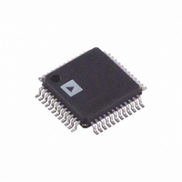
ADUC7032BSTZ-8L-RL Analog Devices Inc, ADUC7032BSTZ-8L-RL Datasheet - Page 82

ADUC7032BSTZ-8L-RL
Manufacturer Part Number
ADUC7032BSTZ-8L-RL
Description
IC,Battery Management,QFP,48PIN,PLASTIC
Manufacturer
Analog Devices Inc
Series
MicroConverter® ADuC7xxxr
Datasheet
1.EVAL-ADUC7032QSPZ.pdf
(116 pages)
Specifications of ADUC7032BSTZ-8L-RL
Core Processor
ARM7
Core Size
16/32-Bit
Speed
20.48MHz
Connectivity
LIN, SPI, UART/USART
Peripherals
POR, PSM, Temp Sensor, WDT
Number Of I /o
9
Program Memory Size
96KB (96K x 8)
Program Memory Type
FLASH
Ram Size
6K x 8
Voltage - Supply (vcc/vdd)
3.5 V ~ 18 V
Data Converters
A/D 2x16b
Oscillator Type
Internal
Operating Temperature
-40°C ~ 105°C
Package / Case
48-LQFP
Lead Free Status / RoHS Status
Lead free / RoHS Compliant
Eeprom Size
-
Lead Free Status / Rohs Status
Compliant
ADuC7032-8L
GPIO Port1 Data Register
Name: GP1DAT
Address: 0xFFFF0D30
Default Value: 0x000000XX
Access: Read/write
Function: This 32-bit MMR configures the direction of the GPIO pins assigned to Port1 (see Table 58). This register also sets the output
value for GPIO pins configured as outputs and reads the status of GPIO pins configured as inputs.
Table 63. GP1DAT MMR Bit Designations
Bit
31 to 26
25
24
23 to 18
17
16
15 to 2
1
0
GPIO Port2 Data Register
Name: GP2DAT
Address: 0xFFFF0D40
Default Value: 0x000000XX
Access: Read/write
Function: This 32-bit MMR configures the direction of the GPIO pins assigned to Port2 (see Table 58). This register also sets the output
value for GPIO pins configured as outputs and reads the status of GPIO pins configured as inputs.
Table 64. GP2DAT MMR Bit Designations
Bit
31
30
29
28
27 to 26
25
24
23
Description
Reserved. This bit is reserved and should be written as 0 by user code.
Port2.6 Direction Select Bit.
Port2.5 Direction Select Bit.
Port2.4 Direction Select Bit.
Reserved. These bits are reserved and should be written as 0 by user code.
Port2.1 Direction Select Bit.
Port2.0 Direction Select Bit.
Reserved. This bit is reserved and should be written as 0 by user code.
Description
Reserved. These bits are reserved and should be written as 0 by user code.
Port1.1 Direction Select Bit.
Port1.0 Direction Select Bit.
Reserved. These bits are reserved and should be written as 0 by user code.
Port1.1 Data Output. The value written to this bit appears directly on the GPIO pin assigned to P1.1.
Port1.0 Data Output. The value written to this bit appears directly on the GPIO pin assigned to P1.0.
Reserved. These bits are reserved and should be written as 0 by user code.
Port1.1 Data Input. This bit is a read-only bit that reflects the current status of the GPIO pin assigned to P1.1. User code should
write 0 to this bit.
Port1.0 Data Input. This bit is a read-only bit that reflects the current status of the GPIO pin assigned to P1.0. User code should
write 0 to this bit.
Cleared to 0 by user code to configure the GPIO pin assigned to P1.1 as an input.
Set to 1 by user code to configure the GPIO pin assigned to P1.1 as an output.
Cleared to 0 by user code to configure the GPIO pin assigned to P1.0 as an input.
Set to 1 by user code to configure the GPIO pin assigned to P1.0 as an output.
Cleared to 0 by user code to configure the GPIO pin assigned to P2.6 as an input.
Set to 1 by user code to configure the GPIO pin assigned to P2.6 as an output.
Cleared to 0 by user code to configure the GPIO pin assigned to P2.5 as an input.
Set to 1 by user code to configure the GPIO pin assigned to P2.5 as an output. This configuration is used to support diagnostic
write capability to the high voltage I/O pins.
Cleared to 0 by user code to configure the GPIO pin assigned to P2.4 as an input. This configuration is used to support
diagnostic readback capability from the high voltage I/O pins (see HVCFG1[2:0]).
Set to 1 by user code to configure the GPIO pin assigned to P2.4 as an output.
Cleared to 0 by user code to configure the GPIO pin assigned to P2.1 as an input.
Set to 1 by user code to configure the GPIO pin assigned to P2.1 as an output.
Cleared to 0 by user code to configure the GPIO pin assigned to P2.0 as an input.
Set to 1 by user code to configure the GPIO pin assigned to P2.0 as an output.
Rev.0 | Page 82 of 116


