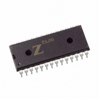
Z84C3006PEG Zilog, Z84C3006PEG Datasheet - Page 34

Z84C3006PEG
Manufacturer Part Number
Z84C3006PEG
Description
IC 6MHZ Z80 CMOS CTC 28-PDIP
Manufacturer
Zilog
Type
Counter/Timer Circuit (CTC)r
Series
Z80r
Specifications of Z84C3006PEG
Frequency
6MHz
Voltage - Supply
4.5 V ~ 5.5 V
Current - Supply
8mA
Operating Temperature
-40°C ~ 100°C
Package / Case
28-DIP (0.600", 15.24mm)
Processor Series
Z84C3xx
Core
Z80
Data Bus Width
8 bit
Maximum Clock Frequency
6 MHz
Operating Supply Voltage
0 V to 5 V
Maximum Operating Temperature
+ 100 C
Mounting Style
Through Hole
Minimum Operating Temperature
- 40 C
Filter Terminals
SMD
Ic Generic Number
84C30
Operating Temperature Min
-40°C
Operating Temperature Max
100°C
Clock Frequency
6MHz
Rohs Compliant
Yes
Cpu Speed
6MHz
Digital Ic Case Style
DIP
No. Of Pins
28
Supply Voltage Range
5V
Operating Temperature Range
-40°C To +100°C
Lead Free Status / RoHS Status
Lead free / RoHS Compliant
Count
-
Lead Free Status / Rohs Status
Details
Other names
269-3910
Z84C3006PEG
Z84C3006PEG
Available stocks
Company
Part Number
Manufacturer
Quantity
Price
Company:
Part Number:
Z84C3006PEG
Manufacturer:
ZILOG
Quantity:
1 980
Company:
Part Number:
Z84C3006PEG
Manufacturer:
Zilog
Quantity:
1 722
Company:
Part Number:
Z84C3006PEG
Manufacturer:
ZILOG
Quantity:
1 980
Company:
Part Number:
Z84C3006PEG
Manufacturer:
WSI
Quantity:
4 970
Part Number:
Z84C3006PEG
Manufacturer:
ZILOG
Quantity:
20 000
- Current page: 34 of 308
- Download datasheet (2Mb)
14
UM008005-0205
Z80 CPU
User’s Manual
Input or Output Cycles
A
D
15
7
MREQ
— D
WAIT
— A
CLK
WR
RD
it can be used directly as a R/W pulse to virtually any type of semiconductor
memory. Furthermore, the WR signal goes inactive one-half T state before
the address and data bus contents are changed so that the overlap
requirements for almost any type of semiconductor memory type is met.
Figure 6.
Figure 7 illustrates an I/O read or I/O write operation. During I/O operations
a single wait state is automatically inserted. The reason is that during I/O
operations, the time from when the IORQ signal goes active until the CPU
must sample the WAIT line is very short. Without this extra state, sufficient
time does not exist for an I/O port to decode its address and activate the
WAIT line if a wait is required. Also, without this wait state, it is difficult to
design MOS I/O devices that can operate at full CPU speed. During this wait
state time, the WAIT request signal is sampled.
During a read I/O operation, the RD line is used to enable the addressed port
onto the data bus just as in the case of a memory read. For I/O write
operations, the WR line is used as a clock to the I/O port.
0
0
Memory Address
Memory Read or Write Cycle
Memory Read Cycle
T
2
In
T
3
T
1
Memory Address
Memory Write Cycle
T
Data Out
2
T
3
Overview
Related parts for Z84C3006PEG
Image
Part Number
Description
Manufacturer
Datasheet
Request
R

Part Number:
Description:
Communication Controllers, ZILOG INTELLIGENT PERIPHERAL CONTROLLER (ZIP)
Manufacturer:
Zilog, Inc.
Datasheet:

Part Number:
Description:
KIT DEV FOR Z8 ENCORE 16K TO 64K
Manufacturer:
Zilog
Datasheet:

Part Number:
Description:
KIT DEV Z8 ENCORE XP 28-PIN
Manufacturer:
Zilog
Datasheet:

Part Number:
Description:
DEV KIT FOR Z8 ENCORE 8K/4K
Manufacturer:
Zilog
Datasheet:

Part Number:
Description:
KIT DEV Z8 ENCORE XP 28-PIN
Manufacturer:
Zilog
Datasheet:

Part Number:
Description:
DEV KIT FOR Z8 ENCORE 4K TO 8K
Manufacturer:
Zilog
Datasheet:

Part Number:
Description:
CMOS Z8 microcontroller. ROM 16 Kbytes, RAM 256 bytes, speed 16 MHz, 32 lines I/O, 3.0V to 5.5V
Manufacturer:
Zilog, Inc.
Datasheet:

Part Number:
Description:
Low-cost microcontroller. 512 bytes ROM, 61 bytes RAM, 8 MHz
Manufacturer:
Zilog, Inc.
Datasheet:

Part Number:
Description:
Z8 4K OTP Microcontroller
Manufacturer:
Zilog, Inc.
Datasheet:

Part Number:
Description:
CMOS SUPER8 ROMLESS MCU
Manufacturer:
Zilog, Inc.
Datasheet:

Part Number:
Description:
SL1866 CMOSZ8 OTP Microcontroller
Manufacturer:
Zilog, Inc.
Datasheet:

Part Number:
Description:
SL1866 CMOSZ8 OTP Microcontroller
Manufacturer:
Zilog, Inc.
Datasheet:

Part Number:
Description:
OTP (KB) = 1, RAM = 125, Speed = 12, I/O = 14, 8-bit Timers = 2, Comm Interfaces Other Features = Por, LV Protect, Voltage = 4.5-5.5V
Manufacturer:
Zilog, Inc.
Datasheet:

Part Number:
Description:
Manufacturer:
Zilog, Inc.
Datasheet:


