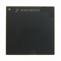
MC68EC060RC50 Freescale Semiconductor, MC68EC060RC50 Datasheet - Page 159

MC68EC060RC50
Manufacturer Part Number
MC68EC060RC50
Description
IC MPU 32BIT 50MHZ 206-PGA
Manufacturer
Freescale Semiconductor
Specifications of MC68EC060RC50
Processor Type
M680x0 32-Bit
Speed
50MHz
Voltage
3.3V
Mounting Type
Surface Mount
Package / Case
206-PGA
Family Name
M68000
Device Core
ColdFire
Device Core Size
32b
Frequency (max)
50MHz
Instruction Set Architecture
RISC
Supply Voltage 1 (typ)
3.3V
Operating Supply Voltage (max)
3.465V
Operating Supply Voltage (min)
3.135V
Operating Temp Range
0C to 110C
Operating Temperature Classification
Commercial
Mounting
Through Hole
Pin Count
206
Package Type
PGA
Lead Free Status / RoHS Status
Contains lead / RoHS non-compliant
Features
-
Lead Free Status / Rohs Status
Compliant
Available stocks
Company
Part Number
Manufacturer
Quantity
Price
Company:
Part Number:
MC68EC060RC50
Manufacturer:
NXP
Quantity:
1 746
- Current page: 159 of 416
- Download datasheet (2Mb)
Bus Operation
of BCLK represent the rising edges of CLK in which CLKEN is asserted. However, there are
cases in which the BCLK concept does not apply.
The BCLK concept does not apply to the IPLx and RSTI input signals. These inputs are sam-
pled every CLK edge. The processor status (PSTx), RSTO, and IPEND outputs do not follow
the BCLK concept, either, since these outputs can change on any CLK rising edge, regard-
less of CLKEN. The BB and TIP signals generally follow the BCLK concept except when
these signals are already driven asserted by the processor and then three-stated. This
occurs when the bus is arbitrated away from the processor immediately after an active bus
cycle. These outputs are actively negated for one CLK period before three-stating. Figure 7-
2, Figure 7-3, and Figure 7-4 illustrate the behavior of BB and TIP in the case mentioned.
The BB signal is not recommended for use in full-speed bus designs since bus contention
is possible when tied to alternate masters’ BB pins.
Other implementations of CLKEN are not supported.
7.3 ACKNOWLEDGE TERMINATION IGNORE STATE CAPABILITY
The MC68060 provides the capability to ignore termination acknowledgments to assist in
system designs. Independent ignore state counters for read and write, primary (initial) trans-
fer, and secondary (burst) transfer are used during bus cycles to determine which BCLK ris-
ing edges transfer acknowledge termination signals should be ignored or sampled.
This special mode is selected during a reset operation. Please refer to 7.14 Special Modes
of Operation for details on how to enable this mode.
7.4 BUS CONTROL REGISTER
The bus control register (BUSCR) is accessed via the MOVEC instruction. Its main purpose
is to provide a way to control the external LOCK and LOCKE signals in software. This fea-
ture is essential in emulating the CAS2 instruction and in providing a means to control bus
arbitration activity during critical code segments. Figure 7-5 shows the BUSCR format.
L—Lock Bit
SL—Shadow Copy, Lock Bit
7-4
0 = Negate external LOCK signal.
1 = Assert external LOCK signal.
0 = LOCK negated sequence at time of exception.
1 = LOCK asserted at time of exception.
31
L
30
SL
LE SLE
29
28
Figure 7-5. Bus Control Register Format
27
M68060 USER’S MANUAL
Reserved for Future Use
0
MOTOROLA
Related parts for MC68EC060RC50
Image
Part Number
Description
Manufacturer
Datasheet
Request
R
Part Number:
Description:
Manufacturer:
Freescale Semiconductor, Inc
Datasheet:
Part Number:
Description:
Manufacturer:
Freescale Semiconductor, Inc
Datasheet:
Part Number:
Description:
Manufacturer:
Freescale Semiconductor, Inc
Datasheet:
Part Number:
Description:
Manufacturer:
Freescale Semiconductor, Inc
Datasheet:
Part Number:
Description:
Manufacturer:
Freescale Semiconductor, Inc
Datasheet:
Part Number:
Description:
Manufacturer:
Freescale Semiconductor, Inc
Datasheet:
Part Number:
Description:
Manufacturer:
Freescale Semiconductor, Inc
Datasheet:
Part Number:
Description:
Manufacturer:
Freescale Semiconductor, Inc
Datasheet:
Part Number:
Description:
Manufacturer:
Freescale Semiconductor, Inc
Datasheet:
Part Number:
Description:
Manufacturer:
Freescale Semiconductor, Inc
Datasheet:
Part Number:
Description:
Manufacturer:
Freescale Semiconductor, Inc
Datasheet:
Part Number:
Description:
Manufacturer:
Freescale Semiconductor, Inc
Datasheet:
Part Number:
Description:
Manufacturer:
Freescale Semiconductor, Inc
Datasheet:
Part Number:
Description:
Manufacturer:
Freescale Semiconductor, Inc
Datasheet:
Part Number:
Description:
Manufacturer:
Freescale Semiconductor, Inc
Datasheet:


