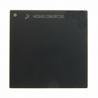
MC68EC060RC50 Freescale Semiconductor, MC68EC060RC50 Datasheet - Page 287

MC68EC060RC50
Manufacturer Part Number
MC68EC060RC50
Description
IC MPU 32BIT 50MHZ 206-PGA
Manufacturer
Freescale Semiconductor
Specifications of MC68EC060RC50
Processor Type
M680x0 32-Bit
Speed
50MHz
Voltage
3.3V
Mounting Type
Surface Mount
Package / Case
206-PGA
Family Name
M68000
Device Core
ColdFire
Device Core Size
32b
Frequency (max)
50MHz
Instruction Set Architecture
RISC
Supply Voltage 1 (typ)
3.3V
Operating Supply Voltage (max)
3.465V
Operating Supply Voltage (min)
3.135V
Operating Temp Range
0C to 110C
Operating Temperature Classification
Commercial
Mounting
Through Hole
Pin Count
206
Package Type
PGA
Lead Free Status / RoHS Status
Contains lead / RoHS non-compliant
Features
-
Lead Free Status / Rohs Status
Compliant
Available stocks
Company
Part Number
Manufacturer
Quantity
Price
Company:
Part Number:
MC68EC060RC50
Manufacturer:
NXP
Quantity:
1 746
- Current page: 287 of 416
- Download datasheet (2Mb)
IEEE 1149.1 Test (JTAG) and Debug Pipe Control Modes
Operating independently of the 5-bit shift register, the 6-bit parallel register is the command
register used by the operand execution pipeline (OEP) control logic to control processor
operations. The sixth bit of the parallel register is connected to the PDISABLE input and
bypasses the 5-bit shift register. PDISABLE should normally be driven negated at all times
to indicate that the command register is active. The other five bits of the parallel register are
each connected to a corresponding bit in the shift register. The PAPPLY input controls the
parallel register. When PAPPLY is asserted, the PDISABLE and shift register data are
latched into the parallel register, and the command is then transmitted to the OEP control
logic. Do not assert both PAPPLY and PSHIFT on the same rising CLK edge as this is inter-
preted as a “no operation”. Do not assert PAPPLY more frequently than once every other
rising CLK edge. Although most commands are five bits in length, it is not necessary to shift
in all five bits for the “generate an emulator interrupt” command. For that command, only
three bits need to be shifted in. Figure 9-11 shows a sample interface timing diagram.
9-26
PARALLEL REGISTER
SERIAL REGISTER 4
SERIAL REGISTER 3
SERIAL REGISTER 2
SERIAL REGISTER 0
SERIAL REGISTER 1
COMMAND VALID
PDISABLE
PAPPLY
PSHIFT
JTAG
PTDI
CLK
0
Figure 9-11. Interface Timing
M68060 USER’S MANUAL
0
1
2
1
0
3
2
0
1
3
4
2
1
0
4
3
2
0
1
0
4
3
2
1
MOTOROLA
Related parts for MC68EC060RC50
Image
Part Number
Description
Manufacturer
Datasheet
Request
R
Part Number:
Description:
Manufacturer:
Freescale Semiconductor, Inc
Datasheet:
Part Number:
Description:
Manufacturer:
Freescale Semiconductor, Inc
Datasheet:
Part Number:
Description:
Manufacturer:
Freescale Semiconductor, Inc
Datasheet:
Part Number:
Description:
Manufacturer:
Freescale Semiconductor, Inc
Datasheet:
Part Number:
Description:
Manufacturer:
Freescale Semiconductor, Inc
Datasheet:
Part Number:
Description:
Manufacturer:
Freescale Semiconductor, Inc
Datasheet:
Part Number:
Description:
Manufacturer:
Freescale Semiconductor, Inc
Datasheet:
Part Number:
Description:
Manufacturer:
Freescale Semiconductor, Inc
Datasheet:
Part Number:
Description:
Manufacturer:
Freescale Semiconductor, Inc
Datasheet:
Part Number:
Description:
Manufacturer:
Freescale Semiconductor, Inc
Datasheet:
Part Number:
Description:
Manufacturer:
Freescale Semiconductor, Inc
Datasheet:
Part Number:
Description:
Manufacturer:
Freescale Semiconductor, Inc
Datasheet:
Part Number:
Description:
Manufacturer:
Freescale Semiconductor, Inc
Datasheet:
Part Number:
Description:
Manufacturer:
Freescale Semiconductor, Inc
Datasheet:
Part Number:
Description:
Manufacturer:
Freescale Semiconductor, Inc
Datasheet:


