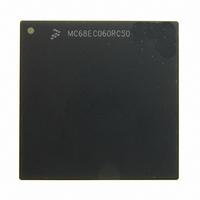
MC68EC060RC50 Freescale Semiconductor, MC68EC060RC50 Datasheet - Page 262

MC68EC060RC50
Manufacturer Part Number
MC68EC060RC50
Description
IC MPU 32BIT 50MHZ 206-PGA
Manufacturer
Freescale Semiconductor
Specifications of MC68EC060RC50
Processor Type
M680x0 32-Bit
Speed
50MHz
Voltage
3.3V
Mounting Type
Surface Mount
Package / Case
206-PGA
Family Name
M68000
Device Core
ColdFire
Device Core Size
32b
Frequency (max)
50MHz
Instruction Set Architecture
RISC
Supply Voltage 1 (typ)
3.3V
Operating Supply Voltage (max)
3.465V
Operating Supply Voltage (min)
3.135V
Operating Temp Range
0C to 110C
Operating Temperature Classification
Commercial
Mounting
Through Hole
Pin Count
206
Package Type
PGA
Lead Free Status / RoHS Status
Contains lead / RoHS non-compliant
Features
-
Lead Free Status / Rohs Status
Compliant
Available stocks
Company
Part Number
Manufacturer
Quantity
Price
Company:
Part Number:
MC68EC060RC50
Manufacturer:
NXP
Quantity:
1 746
- Current page: 262 of 416
- Download datasheet (2Mb)
SECTION 9
IEEE 1149.1 TEST (JTAG) AND
DEBUG PIPE CONTROL MODES
This section describes the IEEE 1149.1 test access port (normal Joint Test Action Group
(JTAG)) mode and the debug pipe control mode, which are available on the MC68060.
9.1 IEEE 1149.1 TEST ACCESS PORT (NORMAL JTAG) MODE
The MC68060 includes dedicated user-accessible test logic that is fully compliant with the
IEEE standard 1149.1-1993 Standard Test Access Port and Boundary Scan Architecture
except in the case where the JTAG architecture and the LPSTOP function interact. This
case is not formally addressed by the standard, but the MC68060 solution is transparent to
the functionality defined by the standard, has the effect of meeting full compatibility to IEEE
1149.1, and has been approved by the IEEE 1149.1 Working Group Committee.
The following description is to be used in conjunction with the supporting IEEE document
listed previously. This section includes the description of those chip-specific items that the
IEEE standard defines as required as well as those items that are specific to the MC68060
implementation.
The MC68060 JTAG test architecture implementation supports circuit board test strategies
that are based on the IEEE standard. This architecture provides access to all of the data and
control pins of the chip from the board-edge connector through the standard four pin test
access port (TAP) plus the additional optional active low TRST reset pin (see Section 2 Sig-
nal Description for a description of TRST). The test logic itself uses a static design and is
entirely independent of the system logic, except where the JTAG mode is subordinate to
another complimentary test mode (see 9.2 Debug Pipe Control Mode ). When placed in the
subordinate mode, the JTAG test logic is placed in reset and the TAP pins are used for alter-
nate purposes in accordance with the rules and restrictions set forth for the use of a JTAG
compliance enable pin.
The MC68060 JTAG implementation provides the capabilities to:
MOTOROLA
1. Perform boundary scan operations to test circuit board electrical continuity,
2. Bypass the MC68060 by reducing the shift register path to a single cell,
3. Sample the MC68060 system pins during operation and transparently shift out the
4. Set the MC68060 output drive pins to fixed logic values while reducing the shift register
5. Protect the MC68060 system output and input pins from backdriving and random
result,
path to a single cell, and
M68060 USER’S MANUAL
9-1
Related parts for MC68EC060RC50
Image
Part Number
Description
Manufacturer
Datasheet
Request
R
Part Number:
Description:
Manufacturer:
Freescale Semiconductor, Inc
Datasheet:
Part Number:
Description:
Manufacturer:
Freescale Semiconductor, Inc
Datasheet:
Part Number:
Description:
Manufacturer:
Freescale Semiconductor, Inc
Datasheet:
Part Number:
Description:
Manufacturer:
Freescale Semiconductor, Inc
Datasheet:
Part Number:
Description:
Manufacturer:
Freescale Semiconductor, Inc
Datasheet:
Part Number:
Description:
Manufacturer:
Freescale Semiconductor, Inc
Datasheet:
Part Number:
Description:
Manufacturer:
Freescale Semiconductor, Inc
Datasheet:
Part Number:
Description:
Manufacturer:
Freescale Semiconductor, Inc
Datasheet:
Part Number:
Description:
Manufacturer:
Freescale Semiconductor, Inc
Datasheet:
Part Number:
Description:
Manufacturer:
Freescale Semiconductor, Inc
Datasheet:
Part Number:
Description:
Manufacturer:
Freescale Semiconductor, Inc
Datasheet:
Part Number:
Description:
Manufacturer:
Freescale Semiconductor, Inc
Datasheet:
Part Number:
Description:
Manufacturer:
Freescale Semiconductor, Inc
Datasheet:
Part Number:
Description:
Manufacturer:
Freescale Semiconductor, Inc
Datasheet:
Part Number:
Description:
Manufacturer:
Freescale Semiconductor, Inc
Datasheet:


