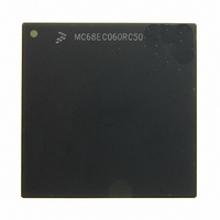
MC68EC060RC50 Freescale Semiconductor, MC68EC060RC50 Datasheet - Page 54

MC68EC060RC50
Manufacturer Part Number
MC68EC060RC50
Description
IC MPU 32BIT 50MHZ 206-PGA
Manufacturer
Freescale Semiconductor
Specifications of MC68EC060RC50
Processor Type
M680x0 32-Bit
Speed
50MHz
Voltage
3.3V
Mounting Type
Surface Mount
Package / Case
206-PGA
Family Name
M68000
Device Core
ColdFire
Device Core Size
32b
Frequency (max)
50MHz
Instruction Set Architecture
RISC
Supply Voltage 1 (typ)
3.3V
Operating Supply Voltage (max)
3.465V
Operating Supply Voltage (min)
3.135V
Operating Temp Range
0C to 110C
Operating Temperature Classification
Commercial
Mounting
Through Hole
Pin Count
206
Package Type
PGA
Lead Free Status / RoHS Status
Contains lead / RoHS non-compliant
Features
-
Lead Free Status / Rohs Status
Compliant
Available stocks
Company
Part Number
Manufacturer
Quantity
Price
Company:
Part Number:
MC68EC060RC50
Manufacturer:
NXP
Quantity:
1 746
- Current page: 54 of 416
- Download datasheet (2Mb)
Signal Description
for one full BCLK cycle and then three-stated one BCLK cycle after the address bus is idled.
If LOCKE was already negated in the BCLK cycle in which the MC68060 relinquishes the
bus, it will be three-stated in the same BCLK cycle the address bus is idled.
LOCKE is provided to help make the MC68060 bus compatible with the MC68040-style bus
protocol; however, for new designs, external bus arbitration logic can be simplified with the
use of BGR instead of LOCKE.
Do not use LOCKE. The LOCKE protocol breaks the integrity of the locked read-modify-
write sequence if it is possible to retry the last write of a read-modify-write operation. The
reason is that when LOCKE is asserted, a bus arbiter can grant the bus to an alternate mas-
ter when the current bus cycle is finished (before the retry is attempted). The bus is arbi-
trated away, the last write’s retry is deferred until the bus is returned to the processor. In the
meantime, the alternate master can access the same location where the write should have
taken place. Hence, the integrity of the locked read-modify-write sequence is compromised
in this situation.
2.3.9 Cache Inhibit Out (CIOUT)
When asserted, this three-state output indicates that the MC68060 will not cache the current
bus information in its internal caches. Refer to Section 4 Memory Management Unit for
more information on CIOUT function. When the MC68060 is not the bus master, the CIOUT
signal is placed in a high-impedance state.
2.3.10 Byte Select Lines (BS3–BS0)
These three-state outputs indicate which bytes within a long-word transfer are being
selected and which bytes of the data bus will be used for the transfer. BS0 refers to D31–
D24, BS1 refers to D23–D16, BS2 refers to D15–D8, and BS3 refers to D7–D0. These sig-
nals are generated to provide byte data select signals which are decoded from the SIZx, A1,
and A0 signals as shown in Table 2-6. These signals are placed in a high-impedance state
when the MC68060 is not the bus master.
2.4 MASTER TRANSFER CONTROL SIGNALS
The following signals provide control functions for bus cycles when the MC68060 is the bus
master. Refer to Section 7 Bus Operation for detailed information about the relationship
of the bus cycle control signals to bus operation.
2-8
Transfer Size
Long Word
Word
Word
Byte
Byte
Byte
Byte
Line
SIZ1
0
0
0
0
1
1
0
1
Table 2-6. Data Bus Byte Select Signals
SIZ0
1
1
1
1
0
0
0
1
M68060 USER’S MANUAL
A1
0
0
1
1
0
1
x
x
A0
0
1
0
1
0
0
x
x
D31–D24
BS0
0
1
1
1
0
1
0
0
D23–D16
BS1
1
0
1
1
0
1
0
0
D15–D8
BS2
1
1
0
1
1
0
0
0
D7–D0
BS3
1
1
1
0
1
0
0
0
MOTOROLA
Related parts for MC68EC060RC50
Image
Part Number
Description
Manufacturer
Datasheet
Request
R
Part Number:
Description:
Manufacturer:
Freescale Semiconductor, Inc
Datasheet:
Part Number:
Description:
Manufacturer:
Freescale Semiconductor, Inc
Datasheet:
Part Number:
Description:
Manufacturer:
Freescale Semiconductor, Inc
Datasheet:
Part Number:
Description:
Manufacturer:
Freescale Semiconductor, Inc
Datasheet:
Part Number:
Description:
Manufacturer:
Freescale Semiconductor, Inc
Datasheet:
Part Number:
Description:
Manufacturer:
Freescale Semiconductor, Inc
Datasheet:
Part Number:
Description:
Manufacturer:
Freescale Semiconductor, Inc
Datasheet:
Part Number:
Description:
Manufacturer:
Freescale Semiconductor, Inc
Datasheet:
Part Number:
Description:
Manufacturer:
Freescale Semiconductor, Inc
Datasheet:
Part Number:
Description:
Manufacturer:
Freescale Semiconductor, Inc
Datasheet:
Part Number:
Description:
Manufacturer:
Freescale Semiconductor, Inc
Datasheet:
Part Number:
Description:
Manufacturer:
Freescale Semiconductor, Inc
Datasheet:
Part Number:
Description:
Manufacturer:
Freescale Semiconductor, Inc
Datasheet:
Part Number:
Description:
Manufacturer:
Freescale Semiconductor, Inc
Datasheet:
Part Number:
Description:
Manufacturer:
Freescale Semiconductor, Inc
Datasheet:


