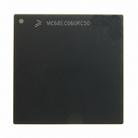
MC68EC060RC50 Freescale Semiconductor, MC68EC060RC50 Datasheet - Page 170

MC68EC060RC50
Manufacturer Part Number
MC68EC060RC50
Description
IC MPU 32BIT 50MHZ 206-PGA
Manufacturer
Freescale Semiconductor
Specifications of MC68EC060RC50
Processor Type
M680x0 32-Bit
Speed
50MHz
Voltage
3.3V
Mounting Type
Surface Mount
Package / Case
206-PGA
Family Name
M68000
Device Core
ColdFire
Device Core Size
32b
Frequency (max)
50MHz
Instruction Set Architecture
RISC
Supply Voltage 1 (typ)
3.3V
Operating Supply Voltage (max)
3.465V
Operating Supply Voltage (min)
3.135V
Operating Temp Range
0C to 110C
Operating Temperature Classification
Commercial
Mounting
Through Hole
Pin Count
206
Package Type
PGA
Lead Free Status / RoHS Status
Contains lead / RoHS non-compliant
Features
-
Lead Free Status / Rohs Status
Compliant
Available stocks
Company
Part Number
Manufacturer
Quantity
Price
Company:
Part Number:
MC68EC060RC50
Manufacturer:
NXP
Quantity:
1 746
- Current page: 170 of 416
- Download datasheet (2Mb)
Clock 2 (C2)
7.7.2 Line Read Transfer
The processor uses line read transfers to access a 16-byte operand for a MOVE16 instruc-
tion and to support cache line filling. A line read accesses a block of four long words, aligned
to a 16-byte memory boundary, by supplying a starting address that points to one of the long
words and requires the memory device to sequentially drive each long word on the data bus.
The selected device must internally increment A3 and A2 of the supplied address for each
transfer, causing the address to wrap around at the end of the block if CLA is not used. Oth-
erwise, the external device may request the processor to increment A3 and A2 in a circular
wrap-around fashion via the CLA input. Refer to 7.7.7 Using CLA to Increment A3 and A2
for details on CLA operation. The address and transfer attributes supplied by the processor
remain stable during the transfers, and the selected device terminates each transfer by driv-
ing the long word on the data bus and asserting TA. A line transfer performed in this manner
with a single address is referred to as a line burst transfer.
The MC68060 supports burst-inhibited line transfers for memory devices that are unable to
support bursting. For this type of bus cycle, the selected device supplies the first long word
pointed to by the processor address and asserts transfer burst inhibit (TBI) with TA for the
first transfer of the line access. The processor responds by terminating the line burst transfer
and accessing the remainder of the line, using three long-word read bus cycles. Although
the selected device can then treat the line bus cycle as four, independent, long-word bus
MOTOROLA
During C2, the processor negates TS. The selected peripheral device uses R/W, SIZ1,
SIZ0, A1, and A0 or BSx to place its information on the data bus. With the exception of
the R/W signal, these signals also select any or all of the operand bytes (D31–D24, D23–
D16, D15–D8, and D7–D0). If the first clock after C1 is not a wait state (CW), then the
selected peripheral device asserts the transfer acknowledge (TA) signal.
The MC68060 implements a special mode called the acknowledge termination ignore
state capability to aid in high-frequency designs. In this mode, the processor begins sam-
pling termination signals such as TA after a user-programmed number of BCLK rising
edges has expired. The SAS signal is provided as a status output to indicate which BCLK
rising edge the processor begins to sample the termination signals. If this mode is dis-
abled, SAS is asserted during C2 to indicate that the processor immediately begins sam-
pling the termination signals. Refer to 7.14.1 Acknowledge Termination Ignore State
Capability for details on this special mode.
Assuming that the acknowledge termination ignore state capability is disabled, at the end
of the first clock cycle C2, the processor samples the level of TA and if asserted, registers
the current value on the data bus; the bus cycle terminates, and the data is passed to the
processor’s appropriate memory unit. If TA is not recognized asserted at the end of the
clock cycle, the processor ignores the data and inserts a wait state instead of terminating
the transfer. The processor continues to sample TA on successive rising edges of BCLK
until TA is recognized asserted. Only when TA is recognized asserted is data passed to
the processor’s appropriate memory unit.
When the processor recognizes TA at the end of a clock cycle and terminates the bus cy-
cle, TIP remains asserted if the processor is ready to begin another bus cycle. Otherwise,
the processor negates TIP during the next clock.
M68060 USER’S MANUAL
Bus Operation
7-15
Related parts for MC68EC060RC50
Image
Part Number
Description
Manufacturer
Datasheet
Request
R
Part Number:
Description:
Manufacturer:
Freescale Semiconductor, Inc
Datasheet:
Part Number:
Description:
Manufacturer:
Freescale Semiconductor, Inc
Datasheet:
Part Number:
Description:
Manufacturer:
Freescale Semiconductor, Inc
Datasheet:
Part Number:
Description:
Manufacturer:
Freescale Semiconductor, Inc
Datasheet:
Part Number:
Description:
Manufacturer:
Freescale Semiconductor, Inc
Datasheet:
Part Number:
Description:
Manufacturer:
Freescale Semiconductor, Inc
Datasheet:
Part Number:
Description:
Manufacturer:
Freescale Semiconductor, Inc
Datasheet:
Part Number:
Description:
Manufacturer:
Freescale Semiconductor, Inc
Datasheet:
Part Number:
Description:
Manufacturer:
Freescale Semiconductor, Inc
Datasheet:
Part Number:
Description:
Manufacturer:
Freescale Semiconductor, Inc
Datasheet:
Part Number:
Description:
Manufacturer:
Freescale Semiconductor, Inc
Datasheet:
Part Number:
Description:
Manufacturer:
Freescale Semiconductor, Inc
Datasheet:
Part Number:
Description:
Manufacturer:
Freescale Semiconductor, Inc
Datasheet:
Part Number:
Description:
Manufacturer:
Freescale Semiconductor, Inc
Datasheet:
Part Number:
Description:
Manufacturer:
Freescale Semiconductor, Inc
Datasheet:


