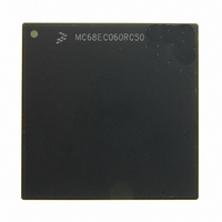
MC68EC060RC50 Freescale Semiconductor, MC68EC060RC50 Datasheet - Page 72

MC68EC060RC50
Manufacturer Part Number
MC68EC060RC50
Description
IC MPU 32BIT 50MHZ 206-PGA
Manufacturer
Freescale Semiconductor
Specifications of MC68EC060RC50
Processor Type
M680x0 32-Bit
Speed
50MHz
Voltage
3.3V
Mounting Type
Surface Mount
Package / Case
206-PGA
Family Name
M68000
Device Core
ColdFire
Device Core Size
32b
Frequency (max)
50MHz
Instruction Set Architecture
RISC
Supply Voltage 1 (typ)
3.3V
Operating Supply Voltage (max)
3.465V
Operating Supply Voltage (min)
3.135V
Operating Temp Range
0C to 110C
Operating Temperature Classification
Commercial
Mounting
Through Hole
Pin Count
206
Package Type
PGA
Lead Free Status / RoHS Status
Contains lead / RoHS non-compliant
Features
-
Lead Free Status / Rohs Status
Compliant
Available stocks
Company
Part Number
Manufacturer
Quantity
Price
Company:
Part Number:
MC68EC060RC50
Manufacturer:
NXP
Quantity:
1 746
- Current page: 72 of 416
- Download datasheet (2Mb)
4.1 MEMORY MANAGEMENT PROGRAMMING MODEL
The memory management programming model is part of the supervisor programming model
for the MC68060. The seven registers that control and provide status information for
address translation in the MC68060 are: the user root pointer register (URP), the supervisor
root pointer register (SRP), the translation control register (TCR), and four independent
transparent translation registers (ITTR0, ITTR1, DTTR0, and DTTR1). Only programs that
execute in the supervisor mode can directly access these registers. Figure 4-2 illustrates the
memory management programming model.
4.1.1 User and Supervisor Root Pointer Registers
The SRP and URP registers each contain the physical address of the translation table’s root,
which the MMU uses for supervisor and user accesses, respectively. The URP points to the
translation table for the current user task. When a new task begins execution, the operating
system typically writes a new root pointer to the URP. A new translation table address
implies that the contents of the ATCs may no longer be valid. Writing a root pointer register
does not affect the contents of the ATCs. A PFLUSH instruction should be executed to flush
the ATCs before loading a new root pointer value, if necessary. Figure 4-3 illustrates the for-
mat of the 32-bit URP and SRP registers. Bits 8–0 of an address loaded into the URP or the
SRP must be zero. Transfers of data to and from these 32-bit registers are long-word trans-
fers.
MOTOROLA
31
31
31
31
31
31
31
31
Figure 4-2. Memory Management Programming Model
Figure 4-3. URP and SRP Register Formats
SUPERVISOR ROOT POINTER
USER ROOT POINTER
M68060 USER’S MANUAL
0
0
0
0
0
0
0
URP
SRP
DTTR0
DTTR1
ITTR0
ITTR1
TCR
USER ROOT POINTER REGISTER
SUPERVISOR ROOT POINTER REGISTER
TRANSLATION CONTROL REGISTER
DATA TRANSPARENT TRANSLATION REGISTER 0
DATA TRANSPARENT TRANSLATION REGISTER 1
INSTRUCTION TRANSPARENT TRANSLATION
REGISTER 0
INSTRUCTION TRANSPARENT TRANSLATION
REGISTER 1
9
8
0
0
Memory Management Unit
0
0
0
0
0
0
0
0
0
0
0
0
0
0
4-3
0
0
0
Related parts for MC68EC060RC50
Image
Part Number
Description
Manufacturer
Datasheet
Request
R
Part Number:
Description:
Manufacturer:
Freescale Semiconductor, Inc
Datasheet:
Part Number:
Description:
Manufacturer:
Freescale Semiconductor, Inc
Datasheet:
Part Number:
Description:
Manufacturer:
Freescale Semiconductor, Inc
Datasheet:
Part Number:
Description:
Manufacturer:
Freescale Semiconductor, Inc
Datasheet:
Part Number:
Description:
Manufacturer:
Freescale Semiconductor, Inc
Datasheet:
Part Number:
Description:
Manufacturer:
Freescale Semiconductor, Inc
Datasheet:
Part Number:
Description:
Manufacturer:
Freescale Semiconductor, Inc
Datasheet:
Part Number:
Description:
Manufacturer:
Freescale Semiconductor, Inc
Datasheet:
Part Number:
Description:
Manufacturer:
Freescale Semiconductor, Inc
Datasheet:
Part Number:
Description:
Manufacturer:
Freescale Semiconductor, Inc
Datasheet:
Part Number:
Description:
Manufacturer:
Freescale Semiconductor, Inc
Datasheet:
Part Number:
Description:
Manufacturer:
Freescale Semiconductor, Inc
Datasheet:
Part Number:
Description:
Manufacturer:
Freescale Semiconductor, Inc
Datasheet:
Part Number:
Description:
Manufacturer:
Freescale Semiconductor, Inc
Datasheet:
Part Number:
Description:
Manufacturer:
Freescale Semiconductor, Inc
Datasheet:


